Datasheet 搜索 > 稳压芯片 > Intersil(英特矽尔) > ISL6217CVZ 数据手册 > ISL6217CVZ 数据手册 7/19 页
 器件3D模型
¥ 36.174
ISL6217CVZ 数据手册 - Intersil(英特矽尔)
制造商:
Intersil(英特矽尔)
分类:
稳压芯片
封装:
TSSOP-38
描述:
精密多相降压PWM精密多相降压PWM定位IMVP- IVA ?? ¢和IMVP -IV Precision Multi-Phase Buck PWM Precision Multi-Phase Buck PWM Positioning IMVP-IV⢠and IMVP-IV
Pictures:
3D模型
符号图
焊盘图
引脚图
产品图
页面导航:
导航目录
ISL6217CVZ数据手册
Page:
of 19 Go
若手册格式错乱,请下载阅览PDF原文件
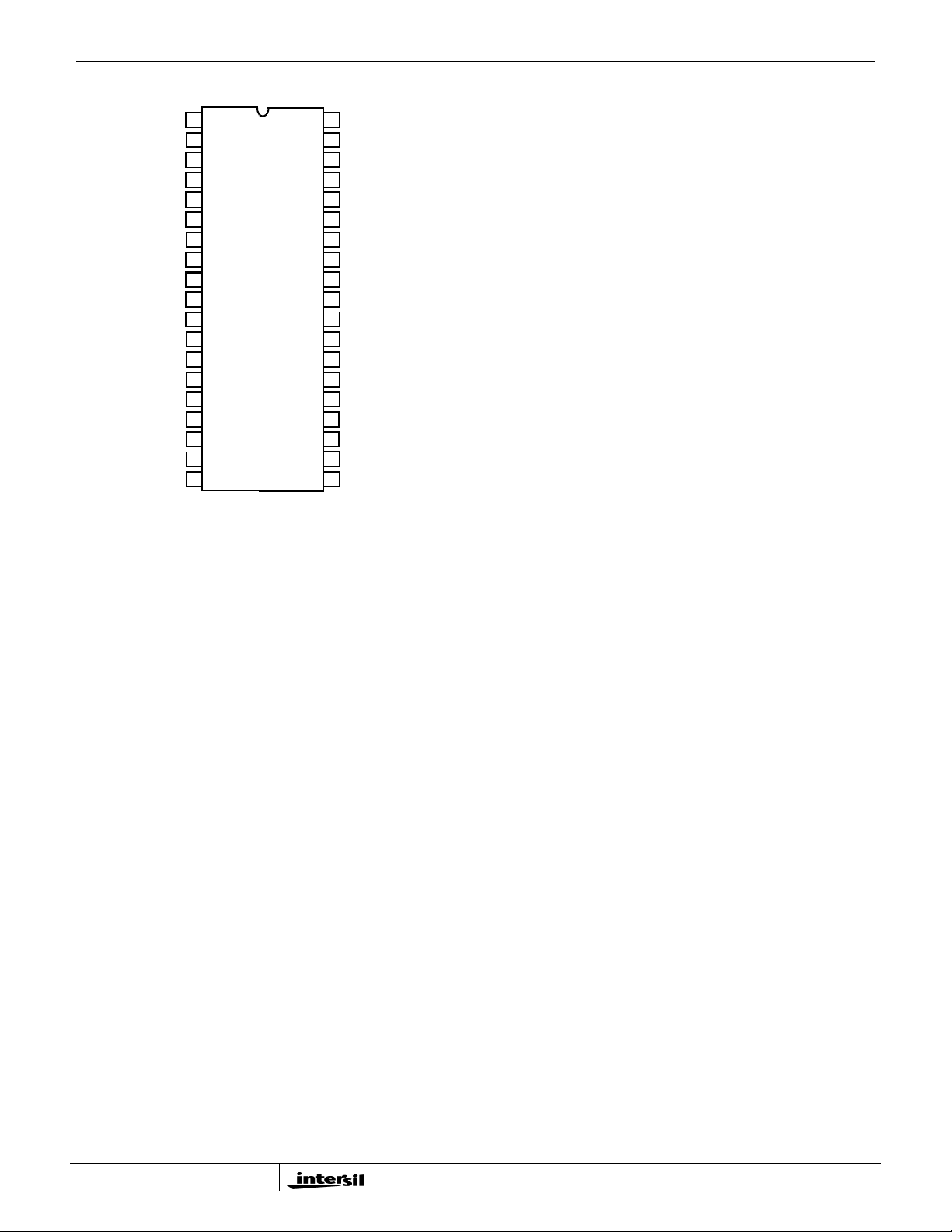
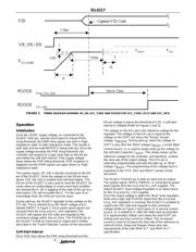
ISL6217
7
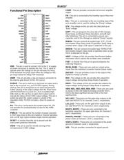
Functional Pin Description
13
1
2
3
4
5
6
7
8
9
10
11
12
14
15
16
17
18
19
VDD
DACOUT
DSV
FSET
PWRCH
EN
DRSEN
DSEN#
VID0
VID1
VID2
VID3
VID4
VID5
PGOOD
EA+
COMP
FB
SOFT
26
38
37
36
35
34
33
32
31
30
29
28
27
25
24
23
22
21
20
VBAT
ISEN1
PHASE1
UG1
BOOT1
VSSP1
LG1
VDDP
LG2
VSSP2
BOOT2
UG2
PHASE2
ISEN2
VSEN
DRSV
STV
OCSET
VSS
ISL6217
TSSOP
VDD - This pin is used to connect +5V to the IC to supply
all power necessary to operate the chip. The IC starts to
operate when the voltage on this pin exceeds the rising
POR threshold and shuts down when the voltage on this
pin drops below the falling POR threshold.
VDDP - This pin provides a low-esr bypass connection to
the internal gate drivers for the +5V source.
PGOOD - This pin is used as an input and an output and is
tied to the Vccp and Vcc_mch PGOOD signals. During
start-up, this pin is recognized as an input and prevents
further slewing of the output voltage from the “Boot” level
until PGOOD from Vccp and Vcc_mch is enabled High.
After start-up, this pin has an open drain output used to
indicate the status of the CORE output voltage. This pin is
pulled low when the system output is outside of the
regulation limits. PGOOD includes a timer for power-on
delay.
EN - This pin is connected to the system signal VR_ON
and provides the enable/disable function for the PWM
controller.
PWRCH - This pin selects the number of power channels.
A HIGH logic level on this pin enables 2 channel operation,
and a LOW logic signal enables single channel operation.
OCSET - A resistor from this pin to ground sets the
overcurrent protection threshold.
VSEN - This pin is used for remote sensing of the
microprocessor CORE voltage.
COMP - This pin provides connection to the error amplifier
output.
FB - This pin is connected to the inverting input of the error
amplifier.
EA+ - This pin is connected to the non-inverting input of the
error amplifier and is used for setting the “Droop” voltage.
STV - The voltage on this pin sets the initial start-up or
“Boot” voltage.
SOFT - This pin programs the slew rate of VID changes,
Deep Sleep and Deeper Sleep transitions and soft-start
after initializing. This pin is connected to ground via a
capacitor, and to EA+ through an external “Droop” resistor.
DSEN# - This pin connects to system logic “STP_CPU#”
and enables Deep Sleep mode of operation. Deep Sleep is
enabled when a logic LOW signal is detected on this pin.
DRSEN - This pin connects to system logic “DPRSLPVR”
and enables Deeper Sleep mode of operation when a logic
HIGH is detected on this pin.
VBAT - Voltage on this pin provides feed-forward battery
information which adjusts the oscillator ramp amplitude.
FSET - A resistor from this pin to ground programs the
switching frequency.
ISEN1, ISEN2 - These pins are used as current sense
inputs from the individual converter channel phase nodes.
DACOUT - This pin provides access to the output of the
Digital-to-Analog Converter.
DSV - The voltage on this pin provides the setpoint for
output voltage during Deep Sleep Mode of operation.
DRSV – The voltage on this pin provides the setpoint for
output voltage during Deeper Sleep Mode of operation.
VID0, VID1, VID2, VID3, VID4, VID5 - These pins are used
as inputs to the 6-bit Digital-to-Analog converter (DAC).
VID0 is the least significant bit and VID5 is the most
significant bit.
UG1, UG2 - These pins are the gate-drive outputs to the
high side MOSFETs for channels 1 and 2, respectively.
LG1, LG2 - These pins are the gate-drive outputs to the
low side MOSFETs for channels 1 and 2, respectively.
BOOT1, BOOT2 - These pins are connected to the
bootstrap capacitors, for upper gate-drive, for channels 1
and 2, respectively.
PHASE1, PHASE2 - These pins are connected to the
phase nodes of channels 1 and 2, respectively.
VSSP1, VSSP2 - These pins are connected to the power
ground of channels 1 and 2, respectively.
VSS - This pin provides connection for signal ground.
器件 Datasheet 文档搜索
AiEMA 数据库涵盖高达 72,405,303 个元件的数据手册,每天更新 5,000 多个 PDF 文件
