Datasheet 搜索 > 负载控制器 > Infineon(英飞凌) > ISO1H811GAUMA1 数据手册 > ISO1H811GAUMA1 数据手册 6/21 页
 器件3D模型
¥ 39.588
ISO1H811GAUMA1 数据手册 - Infineon(英飞凌)
制造商:
Infineon(英飞凌)
分类:
负载控制器
封装:
SOIC-36
描述:
INFINEON ISO1H811GAUMA1 电源负载开关, 电流隔离, 高压侧, 低电平有效, 8路输出, 5.5V, 0.625A, SOIC-36
Pictures:
3D模型
符号图
焊盘图
引脚图
产品图
页面导航:
引脚图在P5P6Hot
典型应用电路图在P4
原理图在P7
封装尺寸在P20
标记信息在P20
功能描述在P8P9P10P11
技术参数、封装参数在P12
应用领域在P8
电气规格在P12P13P14P15P16P17P18P19
导航目录
ISO1H811GAUMA1数据手册
Page:
of 21 Go
若手册格式错乱,请下载阅览PDF原文件
Datasheet 6 Revision 2.5, 2014-10-17
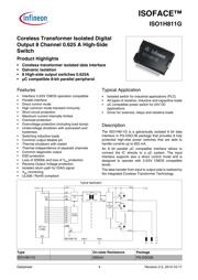
ISOFACE™
ISO1H811G
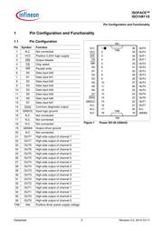
Pin Configuration and Functionality
1.2 Pin Functionality
VCC (Positive 3.3/5V logic supply)
The VCC supplies the input interface that is
galvanically isolated from the output driver stage. The
input interface can be supplied with 3.3/5V.
DIS
(Output disable)
The high-side outputs OUT0...OUT7 can be
immediately switched off by means of the low active pin
DIS
that is an asynchronous signal. The input registers
are also reset by the DIS
signal. The Output remains
switched off after low-high transition of DIS
signal, till
new information is written into the input register.
Current Sink to GNDCC.
CS
(Chip select)
The system microcontroller selects the ISO1H811G by
means of the low active pin CS
to activate the parallel
interface. By connecting the CS
pin and WR pin to
ground the parallel direct control is activated. Current
Source to VCC.
WR
(Parallel write)
In parallel mode data at the input pins (D0 ... D7) are
latched by means of the rising edge of the low active
signal WR
(write). Current Source to VCC.
D0 ... D7 (Data input bit0 ... bit7)
The present data can be latched on the rising edge of
the write signal WR
. D0 ... D7 control the corresponding
output channels OUT0 ...OUT7. By connecting CS
and
WR
to ground, the signals at D0 ... D7 directly control
the outputs. Current Sink to GNDCC.
DIAG
(Common diagnostic output)
The low active DIAG
signal contains the OR-wired
information of the separated overtemperature detection
units for each channel.The output pin DIAG
provides an
open drain functionality. A current source is also
connected to the pin DIAG
. In normal operation the
signal DIAG
is high. When overtemperature or Vbb
below ON-Limit is detected the signal DIAG
changes to
low.
GNDCC (Ground for VCC domain)
This pin acts as the ground reference for the input
interface that is supplied by VCC.
GNDbb (Output driver ground domain)
This pin acts as the ground reference for the output
driver that is supplied by Vbb.
OUT0 ... OUT7 (High side output channel 0 ... 7)
The output high side channels are internally connected
to Vbb and controlled by the corresponding data input
pins D0 ... D7 in parallel mode.
TAB (Vbb, Positive supply for output driver)
The heatslug is connected to the positive supply port of
the output interface.
器件 Datasheet 文档搜索
AiEMA 数据库涵盖高达 72,405,303 个元件的数据手册,每天更新 5,000 多个 PDF 文件
