Datasheet 搜索 > 接口隔离器 > TI(德州仪器) > ISO7140CCDBQR 数据手册 > ISO7140CCDBQR 数据手册 6/32 页
 器件3D模型
¥ 10.91
ISO7140CCDBQR 数据手册 - TI(德州仪器)
制造商:
TI(德州仪器)
分类:
接口隔离器
封装:
SSOP-16
描述:
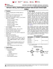
4242 - VPK小尺寸和低功耗三核和四通道数字隔离器 4242-VPK Small-Footprint and Low-Power Triple and Quad Channels Digital Isolators
Pictures:
3D模型
符号图
焊盘图
引脚图
产品图
页面导航:
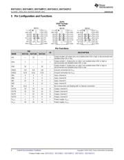
引脚图在P4Hot
典型应用电路图在P21P22P23P24
原理图在P1P16P20
封装尺寸在P27P29P30
标记信息在P27P28
封装信息在P26P27P28P29P30
技术参数、封装参数在P5P17P18
应用领域在P1P21P22P23P24P32
电气规格在P6P7
型号编号列表在P18
导航目录
ISO7140CCDBQR数据手册
Page:
of 32 Go
若手册格式错乱,请下载阅览PDF原文件
ISO7131CC
,
ISO7140CC
,
ISO7140FCC
,
ISO7141CC
,
ISO7141FCC
SLLSE83F –APRIL 2013–REVISED JANUARY 2015
www.ti.com
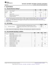
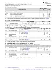
6.4 Thermal Information
ISO7131, ISO714x
THERMAL METRIC
(1)
DBQ UNIT
16 PINS
R
θJA
Junction-to-ambient thermal resistance 104.5 °C/W
R
θJC(top)
Junction-to-case(top) thermal resistance 57.8 °C/W
R
θJB
Junction-to-board thermal resistance 46.8 °C/W
ψ
JT
Junction-to-top characterization parameter 18.3 °C/W
ψ
JB
Junction-to-board characterization parameter 46.4 °C/W
(1) For more information about traditional and new thermal metrics, see the IC Package Thermal Metrics application report, SPRA953.
6.5 Power Dissipation Ratings
TEST CONDITIONS VALUE UNIT
V
CC1
= V
CC2
= 5.5 V, T
J
= 150°C, C
L
= 15 pF
P
D
Device power dissipation 150 mW
Input a 25-MHz, 50% duty cycle square wave
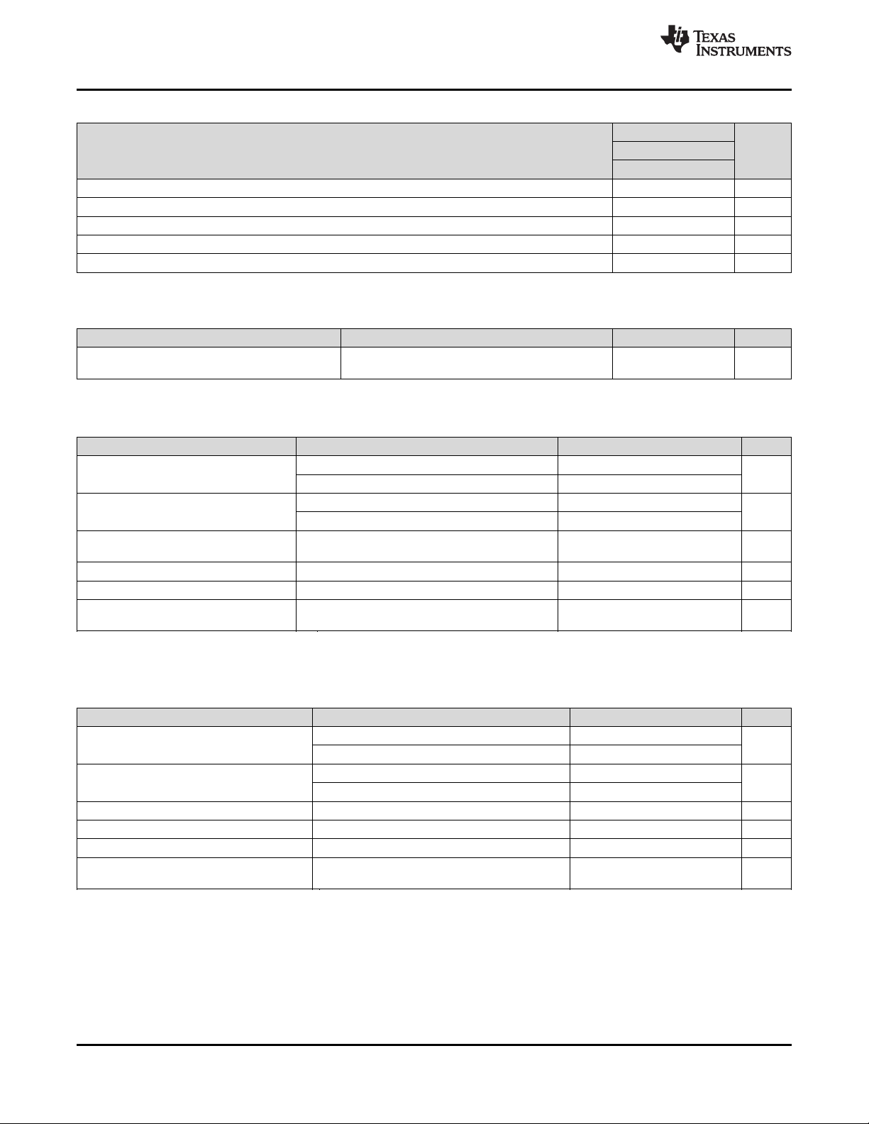
6.6 Electrical Characteristics: V
CC1
and V
CC2
at 5 V ±10%
V
CC1
and V
CC2
at 5 V ± 10% (over recommended operating conditions unless otherwise noted.)
PARAMETER TEST CONDITIONS MIN TYP MAX UNIT
I
OH
= –4 mA; see Figure 10 V
CCO
(1)
– 0.5 4.8
V
OH
High-level output voltage V
I
OH
= –20 μA; see Figure 10 V
CCO
(1)
– 0.1 5
I
OL
= 4 mA; see Figure 10 0.2 0.4
V
OL
Low-level output voltage V
I
OL
= 20 μA; see Figure 10 0 0.1
V
I(HYS)
Input threshold voltage 450 mV
hysteresis
I
IH
High-level input current V
IH
= V
CC
at INx or ENx 10 μA
I
IL
Low-level input current V
IL
= 0 V at INx or ENx –10 μA
Common-mode transient
CMTI V
I
= V
CC
or 0 V; see Figure 13 25 75 kV/μs
immunity
(1) V
CCO
is the supply voltage, V
CC1
or V
CC2
, for the output channel that is being measured.
6.7 Electrical Characteristics: V
CC1
and V
CC2
at 3.3 V ±10%
V
CC1
and V
CC2
at 3.3 V ±10% (over recommended operating conditions unless otherwise noted.)
PARAMETER TEST CONDITIONS MIN TYP MAX UNIT
I
OH
= –4 mA; see Figure 10 V
CCO
(1)
– 0.5 3
V
OH
High-level output voltage V
I
OH
= –20 μA; see Figure 10 V
CCO
(1)
– 0.1 3.3
I
OL
= 4 mA; see Figure 10 0.2 0.4
V
OL
Low-level output voltage V
I
OL
= 20 μA; see Figure 10 0 0.1
V
I(HYS)
Input threshold voltage hysteresis 425 mV
I
IH
High-level input current V
IH
= V
CC
at INx or ENx 10 μA
I
IL
Low-level input current V
IL
= 0 V at INx or ENx –10 μA
Common-mode transient
CMTI V
I
= V
CC
or 0 V; see Figure 13 25 50 kV/μs
immunity
(1) V
CCO
is the supply voltage, V
CC1
or V
CC2
, for the output channel that is being measured.
6 Submit Documentation Feedback Copyright © 2013–2015, Texas Instruments Incorporated
Product Folder Links: ISO7131CC ISO7140CC ISO7140FCC ISO7141CC ISO7141FCC
器件 Datasheet 文档搜索
AiEMA 数据库涵盖高达 72,405,303 个元件的数据手册,每天更新 5,000 多个 PDF 文件
