Datasheet 搜索 > PLC可编程逻辑控制器 > Lattice Semiconductor(莱迪思) > ISPGAL22V10AB-75LJ 数据手册 > ISPGAL22V10AB-75LJ 数据手册 1/16 页
 器件3D模型
¥ 5.62
ISPGAL22V10AB-75LJ 数据手册 - Lattice Semiconductor(莱迪思)
制造商:
Lattice Semiconductor(莱迪思)
分类:
PLC可编程逻辑控制器
封装:
PLCC
Pictures:
3D模型
符号图
焊盘图
引脚图
产品图
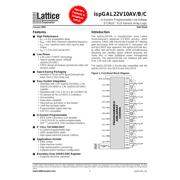
ISPGAL22V10AB-75LJ数据手册
Page:
of 16 Go
若手册格式错乱,请下载阅览PDF原文件
World's
Fastest &
Smallest
SPLD
www.latticesemi.com
1
isp22v10a_02
ispGAL22V10AV/B/C
In-System Programmable Low Voltage
E
2
CMOS
PLD Generic Array Logic
January 2004 Data Sheet
´®
© 2004 Lattice Semiconductor Corp. All Lattice trademarks, registered trademarks, patents, and disclaimers are as listed at www.latticesemi.com/legal. All other
brand or product names are trademarks or registered trademarks of their respective holders. The specifications and information herein are subject to change without
notice.
Features
■
High Performance
•t
PD
= 2.3ns propagation delay
•f
MAX
= 455 MHz maximum operating frequency
•t
CO
= 2ns maximum from clock input to data
output
•t
SU
= 1.3 ns clock set-up time
■
Low Power
• 1.8V core E
2
CMOS
®
technology
•Typical standby power <300µW
(ispGAL22V10AC)
• CMOS design techniques provide low static and
dynamic power
■
Space-Saving Packaging
•Available in 32-pin QFN (Quad Flat-pack No
lead), 5mm x 5mm body size
■
Easy System Integration
• Operation with 3.3V (ispGAL22V10AV), 2.5V
(ispGAL22V10AB) or 1.8V (ispGAL22V10AC)
supplies
• Operation with 3.3V, 2.5V or 1.8V LVCMOS I/O
• 5V tolerant I/O for LVCMOS 3.3 interface
• Hot-socketing
• Open-drain capability
• Input pull-up, pull-down or bus-keeper
• Lead-free package option
• Programmable output slew rate
• 3.3V PCI compatible
■
In-System Programmable
• IEEE 1149.1 boundary scan testable
• 3.3V/2.5V/1.8V in-system programmable
(ISP™) using IEEE 1532 compliant interface
■
E
2
CELL TECHNOLOGY
• In-system programmable logic
• 100% tested/100% yields
• High speed electrical erasure (<50ms)
■
Applications Include
• DMA control
• State machine control
• High speed graphics processing
• Software-driven hardware configuration
■
Boundary Scan USERCODE Register
• Supports electronic signature
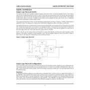
Introduction
The ispGAL22V10A is manufactured using Lattice
Semiconductor’s advanced E
2
CMOS process, which
combines CMOS with Electrically Erasable (E
2
) floating
gate technology. With an advanced E
2
low-power cell
and full CMOS logic approach, the ispGAL22V10A fam-
ily offers fast pin-to-pin speeds, while simultaneously
delivering low standby power without requiring any
“turbo bits” or other traditional power management
schemes. The ispGAL22V10A can interface with both
3.3V, 2.5V and 1.8V signal levels.
The ispGAL22V10A is functionally compatible with the
ispGAL22LV10, GAL22LV10 and GAL22V10.
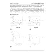
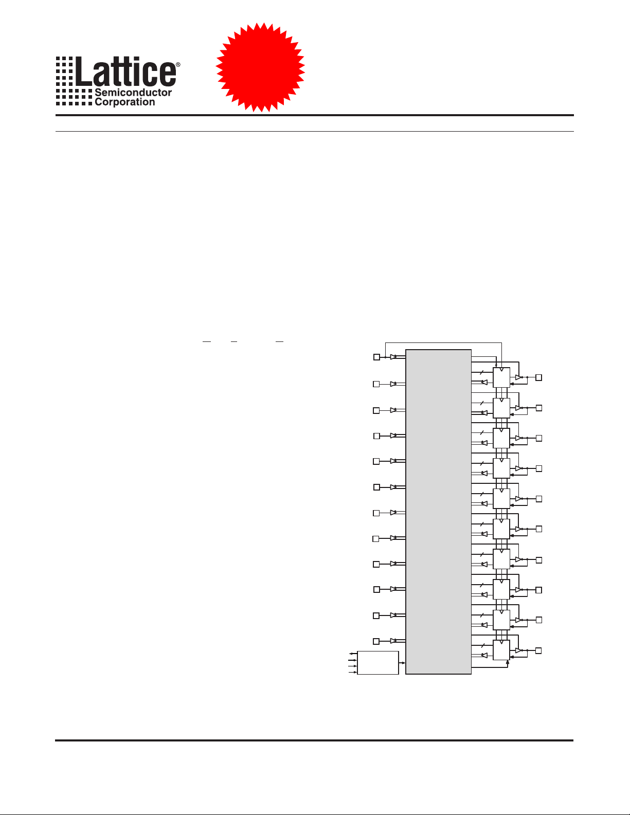
Figure 1. Functional Block Diagram
PROGRAMMABLE
AND-ARRAY
(132X44)
I/O
I/O
I/O
I/O
I/O
I/O
I/O
I/O
I/O
I/O
TDO
TDI
TMS
TCK
I/CLK
I
I
I
I
I
I
I
I
I
I
RESET
PRESET
8
10
12
14
16
16
14
12
10
8
OLMC
OLMC
OLMC
OLMC
OLMC
OLMC
OLMC
OLMC
OLMC
OLMC
PROGRAMMING
LOGIC
I
器件 Datasheet 文档搜索
AiEMA 数据库涵盖高达 72,405,303 个元件的数据手册,每天更新 5,000 多个 PDF 文件
