Datasheet 搜索 > PLC可编程逻辑控制器 > Lattice Semiconductor(莱迪思) > ISPGAL22V10AV-75LJ 数据手册 > ISPGAL22V10AV-75LJ 数据手册 6/16 页
 器件3D模型
¥ 4.974
ISPGAL22V10AV-75LJ 数据手册 - Lattice Semiconductor(莱迪思)
制造商:
Lattice Semiconductor(莱迪思)
分类:
PLC可编程逻辑控制器
封装:
PLCC-28
描述:
SPLD - 简单可编程逻辑器件 PROGRAMMABLE LO VOLT E2CMOS PLD
Pictures:
3D模型
符号图
焊盘图
引脚图
产品图
ISPGAL22V10AV-75LJ数据手册
Page:
of 16 Go
若手册格式错乱,请下载阅览PDF原文件
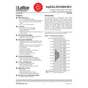
Lattice Semiconductor ispGAL22V10AV/B/C Data Sheet
6
via the parallel port of a PC. Alternatively, the software can output files in formats understood by common auto-
mated test equipment. This equipment can then be used to program ispGAL22V10A devices during the testing of a
circuit board.
Security Bit
A programmable security bit is provided on the ispGAL22V10A devices as a deterrent to unauthorized copying of
the array configuration patterns. Once programmed, this bit defeats readback of the programmed pattern by a
device programmer, securing proprietary designs from competitors. Programming and verification are also
defeated by the security bit. The bit can only be reset by erasing the entire device.
Hot Socketing
The ispGAL22V10A devices are well-suited for applications that require hot socketing. Hot socketing a device
requires that the device, during power-up and down, tolerate active signals on the I/Os and inputs without being
damaged. Additionally, it requires that the effects of I/O pin loading be minimal on active signals. The
ispGAL22V10A devices provide this capability for input voltages in the range of 0V to 3.0V.
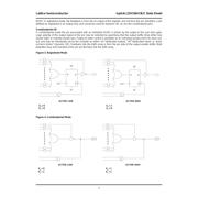
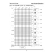
Power-up Reset
Circuitry within the ispGAL22V10A provides a reset signal to all registers during power-up. All internal registers will
have their Q outputs set low after a specified time (tpr, 1µs typical). As a result, the state on the registered output
pins (if they are enabled) will be either high or low on power-up, depending on the programmed polarity of the out-
put pins. This feature can greatly simplify state machine design by providing a known state on power-up. The timing
diagram for power-up is shown above. Because of the asynchronous nature of system power-up, some conditions
must be met to provide a valid power-up reset of the ispGAL22V10A. First, the Vcc rise must be monotonic. Sec-
ond, the clock input must be at static TTL level as shown in the diagram during power up. The registers will reset
within a maximum of tpr time. As in normal system operation, avoid clocking the device until all input and feedback
path setup times have been met. The clock must also meet the minimum pulse width requirements.
Figure 6. Timing Diagram for Power-up
Vcc (min.)
t
pr
Internal Register
Reset to Logic "0"
Device Pin
Reset to Logic "1"
twl
tsu
Device Pin
Reset to Logic "0"
Vcc
CLK
INTERNAL REGISTER
Q - OUTPUT
ACTIVE LOW
OUTPUT REGISTER
ACTIVE HIGH
OUTPUT REGISTER
器件 Datasheet 文档搜索
AiEMA 数据库涵盖高达 72,405,303 个元件的数据手册,每天更新 5,000 多个 PDF 文件
