Datasheet 搜索 > PLC可编程逻辑控制器 > Lattice Semiconductor(莱迪思) > ISPGAL22V10C-10LK 数据手册 > ISPGAL22V10C-10LK 数据手册 1/14 页

¥ 0
ISPGAL22V10C-10LK 数据手册 - Lattice Semiconductor(莱迪思)
制造商:
Lattice Semiconductor(莱迪思)
分类:
PLC可编程逻辑控制器
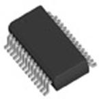
封装:
SOP
Pictures:
3D模型
符号图
焊盘图
引脚图
产品图
页面导航:
导航目录
ISPGAL22V10C-10LK数据手册
Page:
of 14 Go
若手册格式错乱,请下载阅览PDF原文件
ispGAL22V10
In-System Programmable E
2
CMOS PLD
Generic Array Logic™
1
Description
The ispGAL22V10, at 7.5ns maximum propagation delay time,
combines a high performance CMOS process with Electrically Eras-
able (E
2
) floating gate technology to provide the industry's first in-
system programmable 22V10 device. E
2
technology offers high
speed (<100ms) erase times, providing the ability to reprogram or
reconfigure the device quickly and efficiently.
The generic architecture provides maximum design flexibility by al-
lowing the Output Logic Macrocell (OLMC) to be configured by the
user. The ispGAL22V10 is fully function/fuse map/parametric com-
patible with standard bipolar and CMOS 22V10 devices. The stan-
dard PLCC package provides the same functional pinout as the
standard 22V10 PLCC package with No-Connect pins being used
for the ISP interface signals.
Unique test circuitry and reprogrammable cells allow complete AC,
DC, and functional testing during manufacture. As a result, Lat-
tice Semiconductor delivers 100% field programmability and func-
tionality of all GAL products. In addition, 10,000 erase/write cycles
and data retention in excess of 20 years are specified.
Features
• IN-SYSTEM PROGRAMMABLE™ (5-V ONLY)
— 4-Wire Serial Programming Interface
— Minimum 10,000 Program/Erase Cycles
— Built-in Pull-Down on SDI Pin Eliminates Discrete
Resistor on Board (ispGAL22V10C Only)
• HIGH PERFORMANCE E
2
CMOS
®
TECHNOLOGY
— 7.5 ns Maximum Propagation Delay
— Fmax = 111 MHz
—5 ns Maximum from Clock Input to Data Output
— UltraMOS
®
Advanced CMOS Technology
• ACTIVE PULL-UPS ON ALL LOGIC INPUT AND I/O PINS
• COMPATIBLE WITH STANDARD 22V10 DEVICES
— Fully Function/Fuse-Map/Parametric Compatible
with Bipolar and CMOS 22V10 Devices
•E
2
CELL TECHNOLOGY
— In-System Programmable Logic
— 100% Tested/100% Yields
— High Speed Electrical Erasure (<100ms)
— 20 Year Data Retention
• TEN OUTPUT LOGIC MACROCELLS
— Maximum Flexibility for Complex Logic Designs
• APPLICATIONS INCLUDE:
— DMA Control
— State Machine Control
— High Speed Graphics Processing
— Software-Driven Hardware Configuration
• ELECTRONIC SIGNATURE FOR IDENTIFICATION
• LEAD-FREE PACKAGE OPTIONS
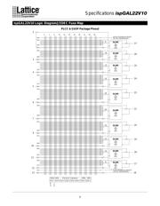
PROGRAMMABLE
AND-ARRAY
(132X44)
I/O/Q
I/O/Q
I/O/Q
I/O/Q
I/O/Q
I/O/Q
I/O/Q
I/O/Q
I/O/Q
I/O/Q
SDO
SDI
MODE
SCLK
I/CLK
I
I
I
I
I
I
I
I
I
I
RESET
PRESET
8
10
12
14
16
16
14
12
10
8
OLMC
OLMC
OLMC
OLMC
OLMC
OLMC
OLMC
OLMC
OLMC
OLMC
PROGRAMMING
LOGIC
I
Copyright © 2004 Lattice Semiconductor Corp. All brand or product names are trademarks or registered trademarks of their respective holders. The specifications and information herein are subject
to change without notice.
LATTICE SEMICONDUCTOR CORP., 5555 Northeast Moore Ct., Hillsboro, Oregon 97124, U.S.A. August 2004
Tel. (503) 268-8000; 1-800-LATTICE; FAX (503) 268-8556; http://www.latticesemi.com
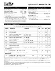
PLCC
SDO
I/O/Q
I/O/Q
I/O/Q
228
I
I
MODE
I
I
I
5
11
14 16
19
25
4
7
9
12 18
21
23
26
I
I/O/Q
I/O/Q
I/O/Q
I
I
I/O/Q
I/CLK
I/O/Q
Vcc
SCLK
I/O/Q
I/O/Q
I
SDI
GND
I
I
Vcc
I/O/Q
I/O/Q
I/O/Q
I/O/Q
I/O/Q
SDO
I/O/Q
I/O/Q
I/O/Q
I/O/Q
I/O/Q
I
SDI
SCLK
I/CLK
I
I
I
I
I
MODE
I
I
I
I
I
GND
1
7
14
28
22
15
ispGAL
22V10
Top View
SSOP
ispGAL22V10
Top View
isp22v10_04
Functional Block Diagram
Pin Configuration
Lead-Free
Package
Options
Available!
器件 Datasheet 文档搜索
AiEMA 数据库涵盖高达 72,405,303 个元件的数据手册,每天更新 5,000 多个 PDF 文件
