Datasheet 搜索 > 电机驱动器 > ST Microelectronics(意法半导体) > L6205PD 数据手册 > L6205PD 数据手册 4/22 页
 器件3D模型
¥ 52.671
L6205PD 数据手册 - ST Microelectronics(意法半导体)
制造商:
ST Microelectronics(意法半导体)
分类:
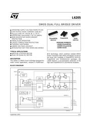
电机驱动器
封装:
SOIC-20
描述:
STMICROELECTRONICS L6205PD 芯片, 电机驱动器, 双路, DMOS, 5.6A, 20PWRSO
Pictures:
3D模型
符号图
焊盘图
引脚图
产品图
页面导航:
导航目录
L6205PD数据手册
Page:
of 22 Go
若手册格式错乱,请下载阅览PDF原文件

L6205
4/21
(6) Also connected at the output drain of the Overcurrent and Thermal protection MOSFET. Therefore, it has to be driven putting in series a
resistor with a value in the range of 2.2kΩ - 180KΩ, recommended 100kΩ
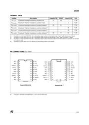
PIN DESCRIPTION
PACKAGE
Name Type Function
SO20/
PowerDIP20
PowerSO20
PIN # PIN #
1 6 IN1
A
Logic Input Bridge A Logic Input 1.
2 7 IN2
A
Logic Input Bridge A Logic Input 2.
3 8 SENSE
A
Power Supply Bridge A Source Pin. This pin must be connected to Power
Ground directly or through a sensing power resistor.
4 9 OUT1
A
Power Output Bridge A Output 1.
5, 6, 15, 16 1, 10, 11,
20
GND GND Signal Ground terminals. In PowerDIP and SO packages,
these pins are also used for heat dissipation toward the
PCB.
7 12 OUT1
B
Power Output Bridge B Output 1.
8 13 SENSE
B
Power Supply Bridge B Source Pin. This pin must be connected to Power
Ground directly or through a sensing power resistor.
9 14 IN1
B
Logic Input Bridge B Logic Input 1.
10 15 IN2
B
Logic Input Bridge B Logic Input 2.
11 16 EN
B
Logic Input
(6)
Bridge B Enable. LOW logic level switches OFF all Power
MOSFETs of Bridge B. This pin is also connected to the
collector of the Overcurrent and Thermal Protection
transistor to implement over current protection.
If not used, it has to be connected to +5V through a
resistor.
12 17 VBOOT Supply
Voltage
Bootstrap Voltage needed for driving the upper
PowerMOSFETs of both Bridge A and Bridge B.
13 18 OUT2
B
Power Output Bridge B Output 2.
14 19 VS
B
Power Supply Bridge B Power Supply Voltage. It must be connected to
the supply voltage together with pin VS
A
.
17 2 VS
A
Power Supply Bridge A Power Supply Voltage. It must be connected to
the supply voltage together with pin VS
B
.
18 3 OUT2
A
Power Output Bridge A Output 2.
19 4 VCP Output Charge Pump Oscillator Output.
20 5 EN
A
Logic Input
(6)
Bridge A Enable. LOW logic level switches OFF all Power
MOSFETs of Bridge A. This pin is also connected to the
collector of the Overcurrent and Thermal Protection
transistor to implement over current protection.
If not used, it has to be connected to +5V through a
resistor.
器件 Datasheet 文档搜索
AiEMA 数据库涵盖高达 72,405,303 个元件的数据手册,每天更新 5,000 多个 PDF 文件
