Datasheet 搜索 > 电机驱动器 > ST Microelectronics(意法半导体) > L6205PD 数据手册 > L6205PD 数据手册 9/22 页
 器件3D模型
¥ 52.671
L6205PD 数据手册 - ST Microelectronics(意法半导体)
制造商:
ST Microelectronics(意法半导体)
分类:
电机驱动器
封装:
SOIC-20
描述:
STMICROELECTRONICS L6205PD 芯片, 电机驱动器, 双路, DMOS, 5.6A, 20PWRSO
Pictures:
3D模型
符号图
焊盘图
引脚图
产品图
页面导航:
导航目录
L6205PD数据手册
Page:
of 22 Go
若手册格式错乱,请下载阅览PDF原文件
9/21
L6205
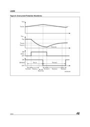
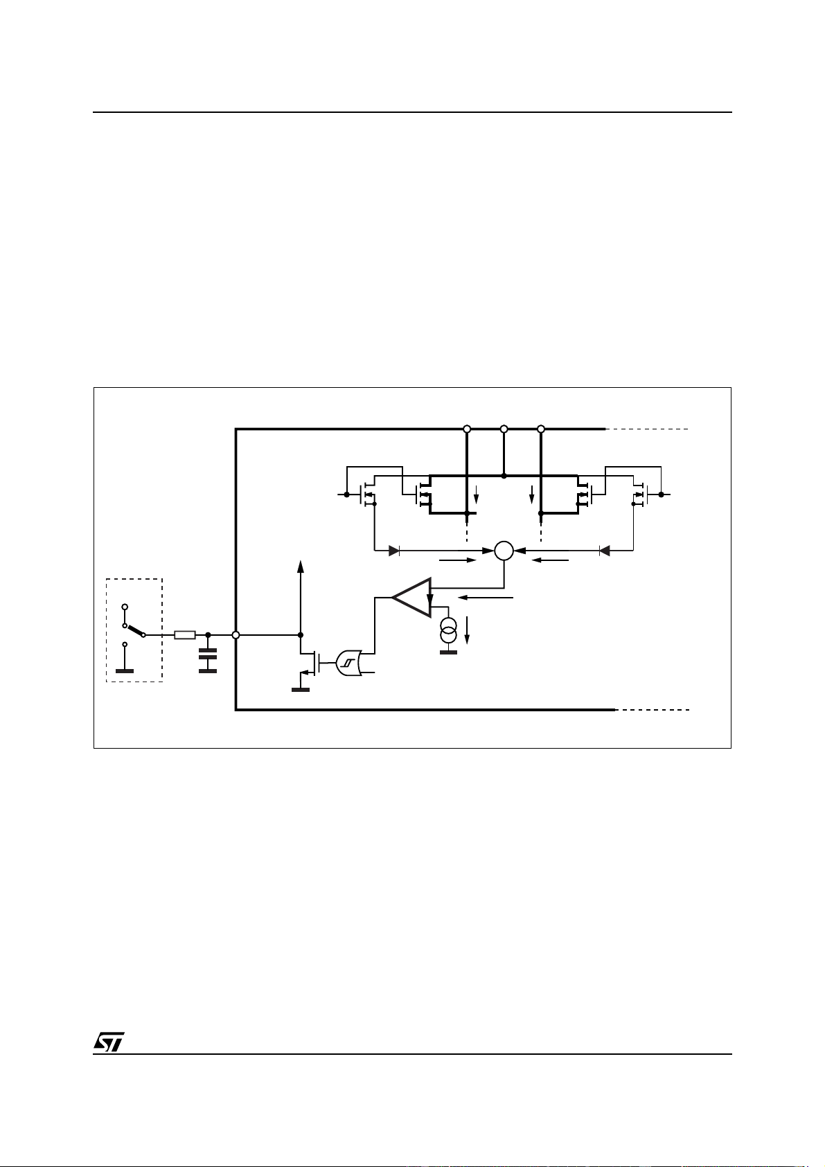
NON-DISSIPATIVE OVERCURRENT PROTECTION
The L6205 integrates an Overcurrent Detection Circuit (OCD). This circuit provides protection against a short
circuit to ground or between two phases of the bridge. With this internal over current detection, the external cur-
rent sense resistor normally used and its associated power dissipation are eliminated. Figure 7 shows a simpli-
fied schematic of the overcurrent detection circuit.
To implement the over current detection, a sensing element that delivers a small but precise fraction of the out-
put current is implemented with each high side power MOS. Since this current is a small fraction of the output
current there is very little additional power dissipation. This current is compared with an internal reference cur-
rent I
REF
. When the output current in one bridge reaches the detection threshold (typically 5.6A) the relative
OCD comparator signals a fault condition. When a fault condition is detected, the EN pin is pulled below the turn
off threshold (1.3V typical) by an internal open drain MOS with a pull down capability of 4mA. By using an ex-
ternal R-C on the EN pin, the off time before recovering normal operation can be easily programmed by means
of the accurate thresholds of the logic inputs.
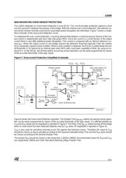
Figure 7. Overcurrent Protection Simplified Schematic
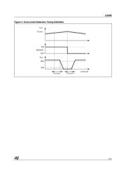
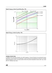
Figure 8 shows the Overcurrent Detection operation. The Disable Time t
DISABLE
before recovering normal opera-
tion can be easily programmed by means of the accurate thresholds of the logic inputs. It is affected whether by
C
EN
and R
EN
values and its magnitude is reported in Figure 9. The Delay Time t
DELAY
before turning off the bridge
when an overcurrent has been detected depends only by C
EN
value. Its magnitude is reported in Figure 10.
C
EN
is also used for providing immunity to pin EN against fast transient noises. Therefore the value of C
EN
should be chosen as big as possible according to the maximum tolerable Delay Time and the R
EN
value should
be chosen according to the desired Disable Time.
The resistor R
EN
should be chosen in the range from 2.2K
Ω
to 180K
Ω
. Recommended values for R
EN
and C
EN
are respectively 100K
Ω
and 5.6nF that allow obtaining 200
µ
s Disable Time.
+
OVER TEMPERATURE
I
REF
(I
1A
+I
2A
) / n
I
1A
/ n
POWER SENSE
1 cell
POWER SENSE
1 cell
POWER DMOS
n cells
POWER DMOS
n cells
HIGH SIDE DMOSs OF
THE BRIDGE A
OUT1
A
OUT2
A
VS
A
I
1A
I
2A
I
2A
/ n
OCD
COMPARATOR
TO GATE
LOGIC
INTERNAL
OPEN-DRAIN
R
DS(ON)
40Ω TYP.
C
EN
R
EN
EN
A
+5V
µC or LOGIC
D02IN1353
器件 Datasheet 文档搜索
AiEMA 数据库涵盖高达 72,405,303 个元件的数据手册,每天更新 5,000 多个 PDF 文件
