Datasheet 搜索 > 电源监控芯片 > ST Microelectronics(意法半导体) > L6599DTR 数据手册 > L6599DTR 数据手册 6/36 页
 器件3D模型
¥ 2.446
L6599DTR 数据手册 - ST Microelectronics(意法半导体)
制造商:
ST Microelectronics(意法半导体)
分类:
电源监控芯片
封装:
SO-16
描述:
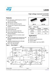
L6599系列 16 V 5 mA 半桥 双端 PWM控制器 - SOIC-16N
Pictures:
3D模型
符号图
焊盘图
引脚图
产品图
页面导航:
导航目录
L6599DTR数据手册
Page:
of 36 Go
若手册格式错乱,请下载阅览PDF原文件
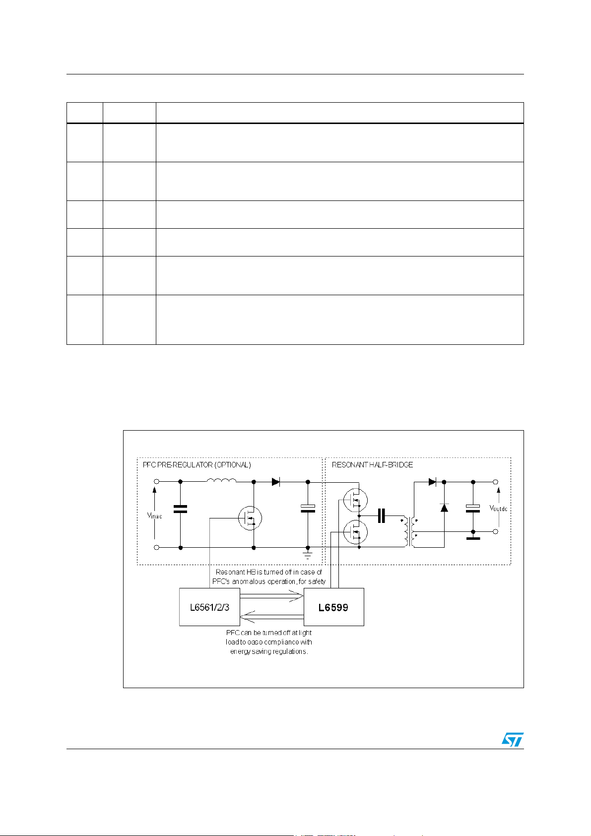
Typical system block diagram L6599
6/36
3 Typical system block diagram
Figure 3. Typical system block diagram
N. Name Function
11 LVG
Low-side gate-drive output. The driver is capable of 0.3 A min. source and 0.8 A min. sink
peak current to drive the lower MOSFET of the half-bridge leg. The pin is actively pulled to
GND during UVLO.
12 V
CC
Supply Voltage of both the signal part of the IC and the low-side gate driver. Sometimes a
small bypass capacitor (0.1 µF typ.) to GND might be useful to get a clean bias voltage for
the signal part of the IC.
13 N.C.
High-voltage spacer. The pin is not internally connected to isolate the high-voltage pin and
ease compliance with safety regulations (creepage distance) on the PCB.
14 OUT
High-side gate-drive floating ground. Current return for the high-side gate-drive current.
Layout carefully the connection of this pin to avoid too large spikes below ground.
15 HVG
High-side floating gate-drive output. The driver is capable of 0.3 A min. source and 0.8A min.
sink peak current to drive the upper MOSFET of the half-bridge leg. A resistor internally
connected to pin 14 (OUT) ensures that the pin is not floating during UVLO.
16 VBOOT
High-side gate-drive floating supply Voltage. The bootstrap capacitor connected between
this pin and pin 14 (OUT) is fed by an internal synchronous bootstrap diode driven in-phase
with the low-side gate-drive. This patented structure replaces the normally used external
diode.
Table 2. Pin functions (continued)
器件 Datasheet 文档搜索
AiEMA 数据库涵盖高达 72,405,303 个元件的数据手册,每天更新 5,000 多个 PDF 文件
