Datasheet 搜索 > 稳压芯片 > TI(德州仪器) > LM2575HVS-12/NOPB 数据手册 > LM2575HVS-12/NOPB 数据手册 4/43 页

¥ 19.853
LM2575HVS-12/NOPB 数据手册 - TI(德州仪器)
制造商:
TI(德州仪器)
分类:
稳压芯片
封装:
TO-263-5
描述:
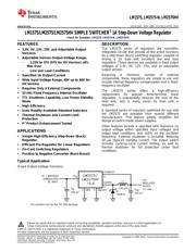
SIMPLE SWITCHER® 降压调节器,LM257x 系列### 直流/直流开关调节器,Texas Instruments用于高达 75V 的宽电压输入设计,以及易用性和灵活性之间的平衡。
Pictures:
3D模型
符号图
焊盘图
引脚图
产品图
页面导航:
典型应用电路图在P1P2P12
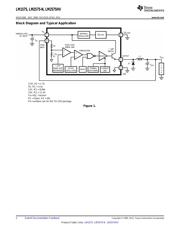
原理图在P2
封装尺寸在P27P28P29P30P31P33P34P35
标记信息在P27P28P29P30P31
封装信息在P27P28P29P30P31P32P33P34P35
技术参数、封装参数在P4P5P6P7P8
应用领域在P1P20P43
电气规格在P4P5P6P7P8P9P10P11P19
型号编号列表在P13P15
导航目录
LM2575HVS-12/NOPB数据手册
Page:
of 43 Go
若手册格式错乱,请下载阅览PDF原文件
LM1575, LM2575-N, LM2575HV
SNVS106E –MAY 1999–REVISED APRIL 2013
www.ti.com
These devices have limited built-in ESD protection. The leads should be shorted together or the device placed in conductive foam
during storage or handling to prevent electrostatic damage to the MOS gates.
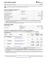
ABSOLUTE MAXIMUM RATINGS
(1)(2)(3)
Maximum Supply Voltage LM1575/LM2575 45V
LM2575HV 63V
ON /OFF Pin Input Voltage −0.3V ≤ V ≤ +V
IN
Output Voltage to Ground (Steady State) −1V
Power Dissipation Internally Limited
Storage Temperature Range −65°C to +150°C
Maximum Junction Temperature 150°C
Minimum ESD Rating (C = 100 pF, R = 1.5 kΩ) 2 kV
Lead Temperature (Soldering, 10 sec.) 260°C
(1) Absolute Maximum Ratings indicate limits beyond which damage to the device may occur. Operating Ratings indicate conditions for
which the device is intended to be functional, but do not ensure specific performance limits. For specified specifications and test
conditions, see Electrical Characteristics.
(2) If Military/Aerospace specified devices are required, please contact the TI Sales Office/ Distributors for availability and specifications.
(3) Refer to RETS LM1575J for current revision of military RETS/SMD.
OPERATING RATINGS
Temperature Range LM1575 −55°C ≤ T
J
≤ +150°C
LM2575/LM2575HV −40°C ≤ T
J
≤ +125°C
Supply Voltage LM1575/LM2575 40V
LM2575HV 60V
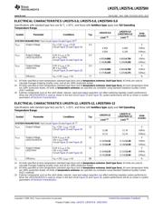
ELECTRICAL CHARACTERISTICS LM1575-3.3, LM2575-3.3, LM2575HV-3.3
Specifications with standard type face are for T
J
= 25°C, and those with boldface type apply over full Operating
Temperature Range .
LM2575-3.3
LM1575-3.3
Units
LM2575HV-3.3
Symbol Parameter Conditions Typ
(Limits)
Limit
(1)
Limit
(2)
SYSTEM PARAMETERS Test Circuit Figure 25 and Figure 26
(3)
V
OUT
Output Voltage V
IN
= 12V, I
LOAD
= 0.2A 3.3 V
Circuit Figure 25 and Figure 26
3.267 3.234 V(Min)
3.333 3.366 V(Max)
V
OUT
Output Voltage 4.75V ≤ V
IN
≤ 40V, 0.2A ≤ I
LOAD
≤ 1A 3.3 V
LM1575/LM2575 Circuit Figure 25 and Figure 26
3.200/3.168 3.168/3.135 V(Min)
3.400/3.432 3.432/3.465 V(Max)
V
OUT
Output Voltage 4.75V ≤ V
IN
≤ 60V, 0.2A ≤ I
LOAD
≤ 1A 3.3 V
LM2575HV Circuit Figure 25 and Figure 26
3.200/3.168 3.168/3.135 V(Min)
3.416/3.450 3.450/3.482 V(Max)
η Efficiency V
IN
= 12V, I
LOAD
= 1A 75 %
(1) All limits specified at room temperature (standard type face) and at temperature extremes (bold type face). All limits are used to
calculate Average Outgoing Quality Level, and all are 100% production tested.
(2) All limits specified at room temperature (standard type face) and at temperature extremes (bold type face). All room temperature limits
are 100% production tested. All limits at temperature extremes are specified via correlation using standard Statistical Quality Control
(SQC) methods.
(3) External components such as the catch diode, inductor, input and output capacitors can affect switching regulator system performance.
When the LM1575/LM2575 is used as shown in the test circuit Figure 25 and Figure 26, system performance will be as shown in system
parameters of Electrical Characteristics.
4 Submit Documentation Feedback Copyright © 1999–2013, Texas Instruments Incorporated
Product Folder Links: LM1575 LM2575-N LM2575HV
器件 Datasheet 文档搜索
AiEMA 数据库涵盖高达 72,405,303 个元件的数据手册,每天更新 5,000 多个 PDF 文件
