Datasheet 搜索 > DC/DC转换器 > TI(德州仪器) > LM2675MX-12 数据手册 > LM2675MX-12 数据手册 6/31 页

 器件3D模型
¥ 18.546
LM2675MX-12 数据手册 - TI(德州仪器)
制造商:
TI(德州仪器)
分类:
DC/DC转换器
封装:
SOIC-8
描述:
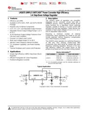
LM2675 SIMPLE SWITCHER电源转换器高效率1A降压电压 LM2675 SIMPLE SWITCHER Power Converter High Efficiency 1A Step-Down Voltage
Pictures:
3D模型
符号图
焊盘图
引脚图
产品图
页面导航:
导航目录
LM2675MX-12数据手册
Page:
of 31 Go
若手册格式错乱,请下载阅览PDF原文件
6
LM2675
SNVS129F –MAY 2004–REVISED JUNE 2016
www.ti.com
Product Folder Links: LM2675
Submit Documentation Feedback Copyright © 2004–2016, Texas Instruments Incorporated
(1) External components such as the catch diode, inductor, input and output capacitors, and voltage programming resistors can affect
switching regulator performance. When the LM2675 is used as shown in Figure 19 test circuits, system performance is as specified by
the system parameters section of Electrical Characteristics.
(2) All limits specified at room temperature and at temperature extremes. All room temperature limits are 100% production tested. All limits
at temperature extremes are specified through correlation using standard Statistical Quality Control (SQC) methods. All limits are used
to calculate Average Outgoing Quality Level (AOQL).
(3) Typical numbers are at 25°C and represent the most likely norm.
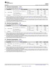
7.8 Electrical Characteristics – Adjustable
T
J
= 25°C (unless otherwise noted; see Figure 19)
(1)
PARAMETER TEST CONDITIONS MIN
(2)
TYP
(3)
MAX
(2)
UNIT
V
FB
Feedback
voltage
V
IN
= 8 V to 40 V, I
LOAD
= 20 mA to 1 A,
V
OUT
programmed for 5 V (see Figure 19)
T
J
= 25°C 1.192 1.21 1.228
V
T
J
= –40°C to 125°C 1.174 1.246
V
IN
= 6.5 V to 40 V, I
LOAD
= 20 mA to 500
mA, V
OUT
programmed for 5 V (see
Figure 19)
T
J
= 25°C 1.192 1.21 1.228
T
J
= –40°C to 125°C 1.174 1.246
η Efficiency V
IN
= 12 V, I
LOAD
= 1 A 90%
(1) All limits specified at room temperature and at temperature extremes. All room temperature limits are 100% production tested. All limits
at temperature extremes are specified through correlation using standard Statistical Quality Control (SQC) methods. All limits are used
to calculate Average Outgoing Quality Level (AOQL).
(2) Typical numbers are at 25°C and represent the most likely norm.
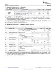
7.9 Electrical Characteristics – All Output Voltage Versions
T
J
= 25°C, V
IN
= 12 V for the 3.3 V, 5 V, and adjustable versions, and V
IN
= 24 V for the 12 V version, and I
LOAD
= 100 mA
(unless otherwise noted)
PARAMETER TEST CONDITIONS MIN
(1)
TYP
(2)
MAX
(1)
UNIT
I
Q
Quiescent current
V
FEEDBACK
= 8 V for 3.3 V, 5 V, and adjustable versions 2.5 3.6 mA
V
FEEDBACK
= 15 V for 12 V versions 2.5 mA
I
STBY
Standby quiescent current ON/OFF Pin = 0 V
T
J
= 25°C 50 100
μA
T
J
= –40°C to 125°C 150
I
CL
Current limit
T
J
= 25°C 1.25 1.55 2.1
A
T
J
= –40°C to 125°C 1.2 2.2
I
L
Output leakage current
V
SWITCH
= 0 V, ON/OFF Pin = 0 V, V
IN
= 40 V 1 25 μA
V
SWITCH
= −1 V, ON/OFF Pin = 0 V 6 15 mA
R
DS(ON)
Switch on-resistance I
SWITCH
= 1 A
T
J
= 25°C 0.25 0.3
Ω
T
J
= –40°C to 125°C 0.5
f
O
Oscillator frequency Measured at switch pin
T
J
= 25°C 260
kHz
T
J
= –40°C to 125°C 225 275
D Minimum duty cycle
T
J
= 25°C 95%
T
J
= –40°C to 125°C 0%
I
BIAS
Feedback bias current V
FEEDBACK
= 1.3 V, adjustable version only 85 nA
V
S/D
ON/OFF pin voltage
T
J
= 25°C 1.4
V
T
J
= –40°C to 125°C 0.8 2
I
S/D
ON/OFF pin current ON/OFF Pin = 0 V
T
J
= 25°C 20
μA
T
J
= –40°C to 125°C 7 37
器件 Datasheet 文档搜索
AiEMA 数据库涵盖高达 72,405,303 个元件的数据手册,每天更新 5,000 多个 PDF 文件
