Datasheet 搜索 > 稳压芯片 > TI(德州仪器) > LM27761DSGR 数据手册 > LM27761DSGR 数据手册 4/27 页

¥ 2.647
LM27761DSGR 数据手册 - TI(德州仪器)
制造商:
TI(德州仪器)
分类:
稳压芯片
封装:
WSON-8
描述:
LM27761DSGR 编带
Pictures:
3D模型
符号图
焊盘图
引脚图
产品图
页面导航:
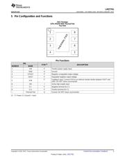
引脚图在P3Hot
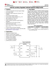
典型应用电路图在P1P5P6P7P8P11
原理图在P9
封装尺寸在P20P22P23
标记信息在P20
封装信息在P19P20P21P22P23
技术参数、封装参数在P4
应用领域在P1
电气规格在P5

导航目录
LM27761DSGR数据手册
Page:
of 27 Go
若手册格式错乱,请下载阅览PDF原文件
4
LM27761
SNVSA85C –OCTOBER 2015–REVISED JANUARY 2017
www.ti.com
Product Folder Links: LM27761
Submit Documentation Feedback Copyright © 2015–2017, Texas Instruments Incorporated
(1) Stresses beyond those listed under Absolute Maximum Ratings may cause permanent damage to the device. These are stress ratings
only, which do not imply functional operation of the device at these or any other conditions beyond those indicated under . Exposure to
absolute-maximum-rated conditions for extended periods may affect device reliability.
(2) If Military/Aerospace specified devices are required, contact the TI Sales Office/Distributors for availability and specifications.
(3) The maximum power dissipation must be de-rated at elevated temperatures and is limited by T
JMAX
(maximum junction temperature), T
A
(ambient temperature) and R
θJA
(junction-to-ambient thermal resistance). The maximum power dissipation at any temperature is:
P
DissMAX
= (T
JMAX
– T
A
)/R
θJA
up to the value listed in the Absolute Maximum Ratings.
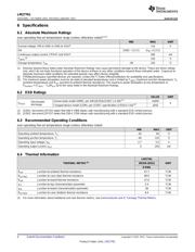
6 Specifications
6.1 Absolute Maximum Ratings
over operating free-air temperature range (unless otherwise noted)
(1)(2)
MIN MAX UNIT
Ground voltage, VIN to GND or GND to VOUT 5.8 V
EN (GND − 0.3 V) (V
IN
+ 0.3 V)
Continuous output current, CPOUT and VOUT 300 mA
T
JMAX
(3)
150 °C
Storage temperature, T
stg
–65 150 °C
(1) JEDEC document JEP155 states that 500-V HBM allows safe manufacturing with a standard ESD control process.
(2) JEDEC document JEP157 states that 250-V CDM allows safe manufacturing with a standard ESD control process.
6.2 ESD Ratings
VALUE UNIT
V
(ESD)
Electrostatic
discharge
Human-body model (HBM), per ANSI/ESDA/JEDEC JS-001
(1)
±1000
V
Charged-device model (CDM), per JEDEC specification JESD22-C101
(2)
±250
6.3 Recommended Operating Conditions
over operating free-air temperature range (unless otherwise noted)
MIN MAX UNIT
Operating ambient temperature, T
A
–40 85 °C
Operating junction temperature, T
J
–40 125 °C
Operating input voltage, V
IN
2.7 5.5 V
Operating output current, I
OUT
0 250 mA
(1) For more information about traditional and new thermal metrics, see Semiconductor and IC Package Thermal Metrics.
6.4 Thermal Information
THERMAL METRIC
(1)
LM27761
UNITWSON (DSG)
8 PINS
R
θJA
Junction-to-ambient thermal resistance 67.7 °C/W
R
θJC(top)
Junction-to-case (top) thermal resistance 89.9 °C/W
R
θJB
Junction-to-board thermal resistance 37.6 °C/W
ψ
JT
Junction-to-top characterization parameter 2.4 °C/W
ψ
JB
Junction-to-board characterization parameter 38 °C/W
R
θJC(bot)
Junction-to-case (bottom) thermal resistance 9.4 °C/W
器件 Datasheet 文档搜索
AiEMA 数据库涵盖高达 72,405,303 个元件的数据手册,每天更新 5,000 多个 PDF 文件
