Datasheet 搜索 > 比较器 > TI(德州仪器) > LM2903M 数据手册 > LM2903M 数据手册 6/29 页
 器件3D模型
¥ 3.291
LM2903M 数据手册 - TI(德州仪器)
制造商:
TI(德州仪器)
分类:
比较器
封装:
SOIC-8
描述:
TEXAS INSTRUMENTS LM2903M 模拟比较器, 双路, 精度, 2, 1.5 µs, ± 1V 至 ± 18V, SOIC, 8 引脚
Pictures:
3D模型
符号图
焊盘图
引脚图
产品图
页面导航:
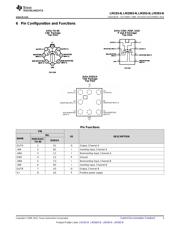
引脚图在P3Hot
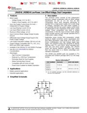
典型应用电路图在P11P12P13P14P15P16P17
原理图在P1P10
封装尺寸在P20P21P23P24
标记信息在P20P21
封装信息在P19P20P21P22P23P24
技术参数、封装参数在P4
应用领域在P1P11P12P13P14P15P16P17P29
电气规格在P4P5P6P7
导航目录
LM2903M数据手册
Page:
of 29 Go
若手册格式错乱,请下载阅览PDF原文件
LM193-N
,
LM2903-N
,
LM293-N
,
LM393-N
SNOSBJ6F –OCTOBER 1999–REVISED DECEMBER 2014
www.ti.com
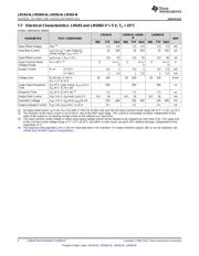
7.7 Electrical Characteristics: LMx93 and LM2903 V
+
= 5 V, T
A
= 25°C
Unless otherwise stated.
LM193-N LM293-N, LM393- LM2903-N
N
PARAMETER TEST CONDITIONS UNIT
MIN TYP MAX MIN TYP MAX MIN TYP MAX
Input Offset Voltage See
(1)
1.0 5.0 1.0 5.0 2.0 7.0 mV
Input Bias Current I
IN
(+) or I
IN
(−) with Output In 25 100 25 250 25 250 nA
Linear Range, V
CM
= 0 V
(2)
Input Offset Current I
IN
(+)−I
IN
(−) V
CM
= 0 V 3.0 25 5.0 50 5.0 50 nA
Input Common Mode V+ = 30 V
(3)
0 V+−1. 0 V+−1 0 V+−1 V
Voltage Range 5 .5 .5
Supply Current R
L
=∞ V
+
=5 V 0.4 1 0.4 1 0.4 1.0 mA
V
+
=36 V 1 2.5 1 2.5 1 2.5 mA
Voltage Gain R
L
≥15 kΩ, V
+
=15 V 50 200 50 200 25 100 V/mV
V
O
= 1 V to 11 V
Large Signal Response V
IN
=TTL Logic Swing, V
REF
=1.4 V 300 300 300 ns
Time V
RL
=5 V, R
L
=5.1 kΩ
Response Time V
RL
=5 V, R
L
=5.1 kΩ
(4)
1.3 1.3 1.5 μs
Output Sink Current V
IN
(−)=1 V, V
IN
(+)=0, V
O
≤1.5 V 6.0 16 6.0 16 6.0 16 mA
Saturation Voltage V
IN
(−)=1 V, V
IN
(+)=0, I
SINK
≤4 mA 250 400 250 400 250 400 mV
Output Leakage Current V
IN
(−)=0, V
IN
(+)=1V, V
O
=5 V 0.1 0.1 0.1 nA
(1) At output switch point, V
O
≃1.4V, R
S
= 0 Ω with V
+
from 5V to 30V; and over the full input common-mode range (0V to V
+
−1.5V), at 25°C.
(2) The direction of the input current is out of the IC due to the PNP input stage. This current is essentially constant, independent of the
state of the output so no loading change exists on the reference or input lines.
(3) The input common-mode voltage or either input signal voltage should not be allowed to go negative by more than 0.3V. The upper end
of the common-mode voltage range is V
+
−1.5 V at 25°C, but either or both inputs can go to 36 V without damage, independent of the
magnitude of V
+
.
(4) The response time specified is for a 100 mV input step with 5 mV overdrive. For larger overdrive signals 300 ns can be obtained, see
LMx93 and LM193A Typical Characteristics .
6 Submit Documentation Feedback Copyright © 1999–2014, Texas Instruments Incorporated
Product Folder Links: LM193-N LM2903-N LM293-N LM393-N
器件 Datasheet 文档搜索
AiEMA 数据库涵盖高达 72,405,303 个元件的数据手册,每天更新 5,000 多个 PDF 文件
