Datasheet 搜索 > 运算放大器 > ST Microelectronics(意法半导体) > LM2904AYDT 数据手册 > LM2904AYDT 数据手册 5/24 页
 器件3D模型
¥ 0.624
LM2904AYDT 数据手册 - ST Microelectronics(意法半导体)
制造商:
ST Microelectronics(意法半导体)
分类:
运算放大器
封装:
SOIC-8
描述:
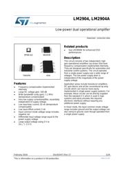
LM2904,LM2904A,LM2904W,低功率,双路双极运算放大器LM2904、LM2904A 和 LM2904W 包含两个独立的运算放大器。 高增益电路采用内部频率补偿,它们设计用于汽车和工业控制系统。 在线性模式下,输入共模电压范围包括接地。宽增益带宽:1.3 MHz 大电压增益:100 dB 每个放大器具有低电源电流:375 μA 单电源工作:+3 V 至 +30 V ### 运算放大器,STMicroelectronics
Pictures:
3D模型
符号图
焊盘图
引脚图
产品图
页面导航:
导航目录
LM2904AYDT数据手册
Page:
of 24 Go
若手册格式错乱,请下载阅览PDF原文件
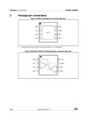
LM2904, LM2904A
Absolute maximum ratings and operating
conditions
DocID2471 Rev 17
5/24
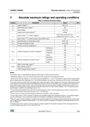
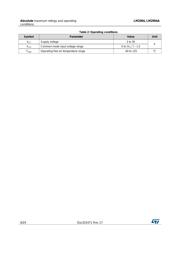
3 Absolute maximum ratings and operating conditions
Table 1: Absolute maximum ratings
Symbol
Parameter
Value
Unit
V
CC
Supply voltage
(1)
±16 or 32
V
V
id
Differential input voltage
(2)
±32
V
in
Input voltage
-0.3 to 32
Output short-circuit duration
(3)
Infinite
s
I
in
Input current
(4)
: V
in
driven negative
5 mA in DC or 50 mA in AC,
(duty cycle = 10 %, T = 1 s)
mA
Input current
(5)
: V
in
driven positive above AMR value
0.4
T
oper
Operating free-air temperature range
-40 to 125
°C
T
stg
Storage temperature range
-65 to 150
T
j
Maximum junction temperature
150
R
thja
Thermal resistance junction to ambient
(6)
DFN8 2x2
57
°C/W
MiniSO8
190
TSSOP8
120
SO8
125
R
thjc
Thermal resistance junction to case
(6)
MiniSO8
39
TSSOP8
37
SO8
40
ESD
HBM: human body model
(7)
300
V
MM: machine model
(8)
200
CDM: charged device model
(9)
1.5
kV
Notes:
(1)
All voltage values, except differential voltage are with respect to network ground terminal.
(2)
Differential voltages are the non-inverting input terminal with respect to the inverting input terminal.
(3)
Short-circuits from the output to V
CC
can cause excessive heating if (V
cc
+
) > 15 V. The maximum output current is approximately
40 mA, independent of the magnitude of V
CC
. Destructive dissipation can result from simultaneous short-circuits on all amplifiers.
(4)
This input current only exists when the voltage at any of the input leads is driven negative. It is due to the collector-base junction
of the input PNP transistor becoming forward-biased and thereby acting as an input diode clamp. In addition to this diode action,
there is NPN parasitic action on the IC chip. This transistor action can cause the output voltages of the op amps to go to the V
CC
voltage level (or to ground for a large overdrive) for the time during which an input is driven negative. This is not destructive and
normal output is restored for input voltages above -0.3 V.
(5)
The junction base/substrate of the input PNP transistor polarized in reverse must be protected by a resistor in series with the
inputs to limit the input current to 400 µA max (R = (V
in
- 32 V)/400 µA).
(6)
Short-circuits can cause excessive heating and destructive dissipation. Values are typical.
(7)
Human body model: a 100 pF capacitor is charged to the specified voltage, then discharged through a 1.5 kΩ resistor between
two pins of the device. This is done for all couples of connected pin combinations while the other pins are floating.
(8)
Machine model: a 200 pF capacitor is charged to the specified voltage, then discharged directly between two pins of the device
with no external series resistor (internal resistor < 5 Ω). This is done for all couples of connected pin combinations while the other
pins are floating.
(9)
Charged device model: all pins and the package are charged together to the specified voltage and then discharged directly to
the ground through only one pin. This is done for all pins.
器件 Datasheet 文档搜索
AiEMA 数据库涵盖高达 72,405,303 个元件的数据手册,每天更新 5,000 多个 PDF 文件
