Datasheet 搜索 > 稳压芯片 > TI(德州仪器) > LM2940S-5.0/NOPB 数据手册 > LM2940S-5.0/NOPB 数据手册 4/37 页

¥ 14.268
LM2940S-5.0/NOPB 数据手册 - TI(德州仪器)
制造商:
TI(德州仪器)
分类:
稳压芯片
封装:
TO-263-4
描述:
TEXAS INSTRUMENTS LM2940S-5.0/NOPB 固定电压稳压器, LDO, 0V至26V, 500mV压差, 5V输出, 1A输出, TO-263-3
Pictures:
3D模型
符号图
焊盘图
引脚图
产品图
页面导航:
引脚图在P3Hot
典型应用电路图在P15
原理图在P1P13
封装尺寸在P21P22P23P24P26P27P28P29
标记信息在P21P22P23P24P25
封装信息在P20P21P22P23P24P25P26P27P28P29
技术参数、封装参数在P4P18
应用领域在P1P37
电气规格在P4P5P6P7P8P18
导航目录
LM2940S-5.0/NOPB数据手册
Page:
of 37 Go
若手册格式错乱,请下载阅览PDF原文件
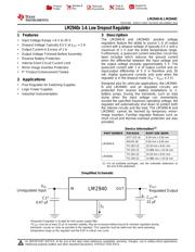
LM2940-N
,
LM2940C
SNVS769J –MARCH 2000–REVISED DECEMBER 2014
www.ti.com
6 Specifications
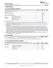
6.1 Absolute Maximum Ratings
(1)(2)
MIN MAX UNIT
LM2940-N KTT, NDE, DCY ≤ 100 ms 60
V
LM2940C KTT, NDE ≤ 1 ms 45
Internally
Internal power dissipation
(3)
Limited
Maximum junction temperature 150
TO-220 (NDE), Wave (10 s) 260
Soldering
DDPAK/TO-263 (KTT) (30 s) 235
temperature
(4)
°C
SOT-223 (DCY) (30 s) 260
WSON-8 (NGN) (30 s) 235
Storage temperature, T
stg
−65 150
(1) Absolute Maximum Ratings are limits beyond which damage to the device may occur. Recommended Operating Conditions are
conditions under which the device functions but the specifications might not be ensured. For ensured specifications and test conditions
see the Electrical Characteristics (5 V and 8 V).
(2) If Military/Aerospace specified devices are required, please contact the Texas Instruments Sales Office/ Distributors for availability and
specifications.
(3) The maximum allowable power dissipation is a function of the maximum junction temperature, T
J
, the junction-to-ambient thermal
resistance, R
θJA
, and the ambient temperature, T
A
. Exceeding the maximum allowable power dissipation will cause excessive die
temperature, and the regulator will go into thermal shutdown. The value of R
θJA
(for devices in still air with no heatsink) is 23.3°C/W for
the TO-220 package, 40.9°C/W for the DDPAK/TO-263 package, and 59.3°C/W for the SOT-223 package. The effective value of R
θJA
can be reduced by using a heatsink (see Heatsinking for specific information on heatsinking). The value of R
θJA
for the WSON package
is specifically dependent on PCB trace area, trace material, and the number of layers and thermal vias. For improved thermal resistance
and power dissipation for the WSON package, refer to Application Note AN-1187 Leadless Leadframe Package (LLP) (SNOA401). It is
recommended that 6 vias be placed under the center pad to improve thermal performance.
(4) Refer to JEDEC J-STD-020C for surface mount device (SMD) package reflow profiles and conditions. Unless otherwise stated, the
temperature and time are for Sn-Pb (STD) only.
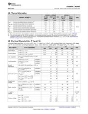
6.2 ESD Ratings
VALUE UNIT
V
(ESD)
Electrostatic discharge Human-body model (HBM), per ANSI/ESDA/JEDEC JS-001
(1)
±2000 V
(1) JEDEC document JEP155 states that 500-V HBM allows safe manufacturing with a standard ESD control process.
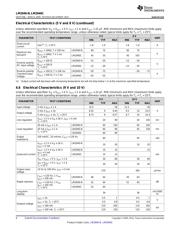
6.3 Recommended Operating Conditions
over operating free-air temperature range (unless otherwise noted)
MIN MAX UNIT
Input voltage 6 26 V
LM2940-N NDE, LM2940-N KTT −40 125
LM2940C NDE, LM2940C KTT 0 125
Temperature
°C
LM2940-N DCY −40 85
LM2940-N NGN −40 125
4 Submit Documentation Feedback Copyright © 2000–2014, Texas Instruments Incorporated
Product Folder Links: LM2940-N LM2940C
器件 Datasheet 文档搜索
AiEMA 数据库涵盖高达 72,405,303 个元件的数据手册,每天更新 5,000 多个 PDF 文件
