Datasheet 搜索 > 稳压芯片 > TI(德州仪器) > LM2941S 数据手册 > LM2941S 数据手册 5/29 页

¥ 6.065
LM2941S 数据手册 - TI(德州仪器)
制造商:
TI(德州仪器)
分类:
稳压芯片
封装:
TO-263-6
描述:
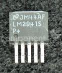
TEXAS INSTRUMENTS LM2941S 电压稳压器, LDO, 可调, -15V至26V输入, 500mV压差, 5V至20V/1A输出, TO-263-5
Pictures:
3D模型
符号图
焊盘图
引脚图
产品图
页面导航:
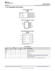
引脚图在P3Hot
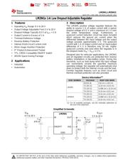
典型应用电路图在P6P12
原理图在P1P10
封装尺寸在P20P21P22P23
标记信息在P20P21
封装信息在P19P20P21P22P23
技术参数、封装参数在P4
应用领域在P1P29
电气规格在P5P6P16

导航目录
LM2941S数据手册
Page:
of 29 Go
若手册格式错乱,请下载阅览PDF原文件
LM2941
,
LM2941C
www.ti.com
SNVS770I –JUNE 1999–REVISED JANUARY 2015
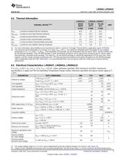
6.4 Thermal Information
LM2941LD LM2941S, LM2941T
WSON TO-263 TO-220
THERMAL METRIC
(1)(2)
UNIT
(NGN) (KTT) (KC)
8 PINS 5 PINS 5 PINS
R
θJA
Junction-to-ambient thermal resistance 40.5 41 32.1
R
θJC(top)
Junction-to-case (top) thermal resistance 26.2 43.2 25.6
R
θJB
Junction-to-board thermal resistance 17 22.9 18.3
°C/W
ψ
JT
Junction-to-top characterization parameter 0.2 11.4 8.5
ψ
JB
Junction-to-board characterization parameter 17.2 21.9 17.7
R
θJC(bot)
Junction-to-case (bottom) thermal resistance 3.2 0.9 0.7
(1) For more information about traditional and new thermal metrics, see the IC Package Thermal Metrics application report, SPRA953.
(2) The maximum power dissipation is a function of T
J
(max), R
θJA
, and T
A
. The maximum allowable power dissipation at any ambient
temperature is P
D
= (T
J
(max) − T
A
)/R
θJA
. If this dissipation is exceeded, the die temperature will rise above 150°C and the LM2941 will
go into thermal shutdown. If the TO-263 package is used, the thermal resistance can be reduced by increasing the PC board copper
area thermally connected to the package. The value R
θJA
for the WSON package is specifically dependent on PCB trace area, trace
material, and the number of layers and thermal vias. For improved thermal resistance and power dissipation for the WSON package,
refer to Application Note AN-1187 (SNOA401). It is recommended that 6 vias be placed under the center pad to improve thermal
performance.
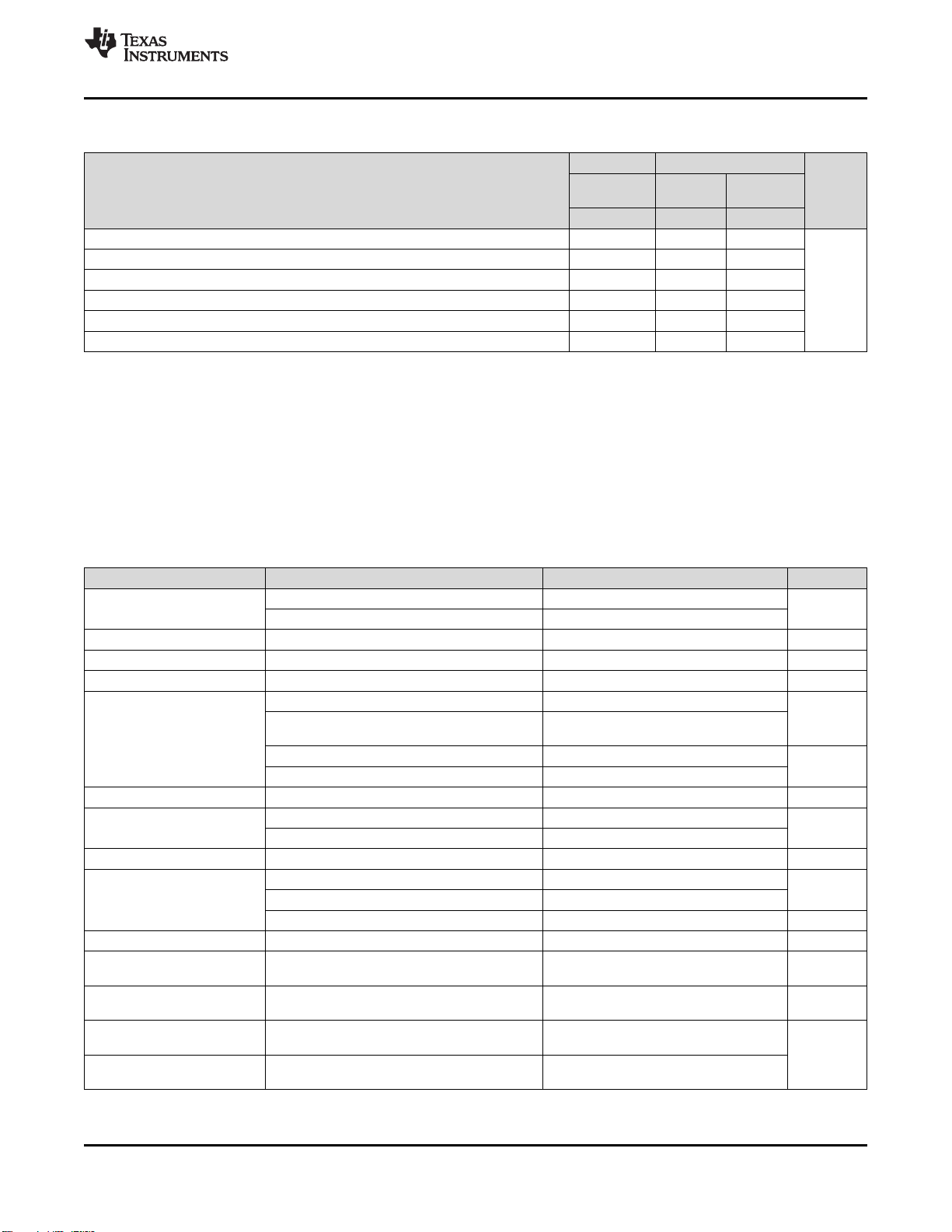
6.5 Electrical Characteristics: LM2941T, LM2941S, LM2941LD
5 V ≤ V
OUT
≤ 20 V, V
IN
= V
OUT
+ 5 V, C
OUT
= 22 μF, unless otherwise specified. MIN (minimum) and MAX (maximum)
specifications in apply over the full Operating Temperature Range (unless otherwise specified) and typical values apply at T
J
= 25°C.
PARAMETER TEST CONDITIONS MIN TYP MAX UNIT
5 mA ≤ I
OUT
≤ 1 A
(1)
1.211 1.275 1.339
Reference voltage V
5 mA ≤ I
OUT
≤ 1 A
(1)
, T
J
= 25°C 1.237 1.275 1.313
Line regulation V
OUT
+ 2 V ≤ V
IN
≤ 26 V, I
OUT
= 5 mA 4 10 mV/V
Load regulation 50 mA ≤ I
OUT
≤ 1 A 7 10 mV/V
Output impedance 100 mADC and 20 mArms, ƒ
OUT
= 120 Hz 7 mΩ/V
V
OUT
+ 2 V ≤ V
IN
< 26 V, I
OUT
= 5 mA 10 20
mA
V
OUT
+ 2 V ≤ V
IN
< 26 V, I
OUT
= 5 mA, T
J
=
10 15
25°C
Quiescent current
V
IN
= V
OUT
+ 5 V, I
OUT
= 1 A 30 60
mA
V
IN
= V
OUT
+ 5 V, I
OUT
= 1 A, T
J
= 25°C 30 45
RMS output noise, % of V
OUT
10 Hz to 100 kHz, I
OUT
= 5 mA 0.003%
ƒ
OUT
= 120 Hz, 1 Vrms, I
L
= 100 mA 0.005 0.04
Ripple rejection %/V
ƒ
OUT
= 120 Hz, 1 Vrms, I
L
= 100 mA, T
J
= 25°C 0.005 0.02
Long-term stability 0.4 %/1000 Hr
I
OUT
= 1 A 0.5 1
V
Dropout voltage I
OUT
= 1 A, T
J
= 25°C 0.5 0.8
I
OUT
= 100 mA 110 200 mV
Short-circuit current V
IN
max = 26 V
(2)
1.6 1.9 A
V
OUT
max 1 V above nominal V
OUT
75
Maximum line transient 60 V
R
OUT
= 100 Ω, t ≤ 100 ms
Maximum operational input
26 31 V
DC
voltage
Reverse polarity
R
OUT
= 100 Ω, V
OUT
≥ −0.6 V −15 −30
DC input voltage
V
Reverse polarity
t ≤ 100 ms, R
OUT
= 100 Ω −50 −75
transient input voltage
(1) The output voltage range is 5 V to 20 V and is determined by the two external resistors, R1 and R2. See Figure 18.
(2) Output current capability will decrease with increasing temperature, but will not go below 1 A at the maximum specified temperatures.
Copyright © 1999–2015, Texas Instruments Incorporated Submit Documentation Feedback 5
Product Folder Links: LM2941 LM2941C
器件 Datasheet 文档搜索
AiEMA 数据库涵盖高达 72,405,303 个元件的数据手册,每天更新 5,000 多个 PDF 文件
