Datasheet 搜索 > 稳压芯片 > ON Semiconductor(安森美) > LM317MABTG 数据手册 > LM317MABTG 数据手册 1/14 页

¥ 4.254
LM317MABTG 数据手册 - ON Semiconductor(安森美)
制造商:
ON Semiconductor(安森美)
分类:
稳压芯片
封装:
TO-220-3
描述:
ON SEMICONDUCTOR LM317MABTG 稳压器
Pictures:
3D模型
符号图
焊盘图
引脚图
产品图
页面导航:
导航目录
LM317MABTG数据手册
Page:
of 14 Go
若手册格式错乱,请下载阅览PDF原文件

© Semiconductor Components Industries, LLC, 2014
August, 2014 − Rev. 24
1 Publication Order Number:
LM317M/D
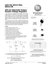
LM317M, NCV317MA,
NCV317M
500 mA Adjustable Output,
Positive Voltage Regulator
The LM317M is an adjustable three−terminal positive voltage
regulator capable of supplying in excess of 500 mA over an output
voltage range of 1.2 V to 37 V. This voltage regulator is exceptionally
easy to use and requires only two external resistors to set the output
voltage. Further, it employs internal current limiting, thermal
shutdown and safe area compensation, making it essentially blow−out
proof.
The LM317M serves a wide variety of applications including local,
on−card regulation. This device also makes an especially simple
adjustable switching regulator, a programmable output regulator, or by
connecting a fixed resistor between the adjustment and output, the
LM317M can be used as a precision current regulator.
Features
• Output Current in Excess of 500 mA
• Output Adjustable between 1.2 V and 37 V
• Internal Thermal Overload Protection
• Internal Short Circuit Current Limiting
• Output Transistor Safe−Area Compensation
• Floating Operation for High Voltage Applications
• Eliminates Stocking Many Fixed Voltages
• NCV Prefix for Automotive and Other Applications Requiring
Unique Site and Control Change Requirements; AEC−Q100
Qualified and PPAP Capable
• These are Pb−Free Devices
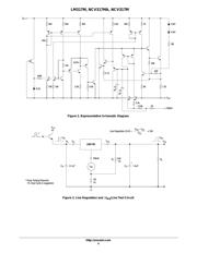
Figure 1. Simplified Application
* = C
in
is required if regulator is located an appreciable distance from power supply filter.
** = C
O
is not needed for stability, however, it does improve transient response.
Since I
Adj
is controlled to less than 100 mA, the error associated with this
term is negligible in most applications.
LM317M
V
in
V
out
R
1
240
R
2
Adjust
I
Adj
*
C
in
0.1mF
**
+
C
O
1.0mF
V
in
V
out
V
out
+ 1.25V
ǒ
1 )
R
2
R
1
Ǔ
) I
Adj
R
2
TO−220AB
T SUFFIX
CASE 221AB
1
2
3
PIN ASSIGNMENT
1
2
3V
in
Adjust
V
out
ORDERING INFORMATION
See detailed ordering and shipping information in the package
dimensions section on page 10 of this data sheet.
1
2
3
Heatsink Surface (shown as terminal 4 in
case outline drawing) is connected to Pin 2.
SOT−223
ST SUFFIX
CASE 318E
DPAK
DT SUFFIX
CASE 369C
Heatsink surface
connected to Pin 2
http://onsemi.com
1
2
3
4
See general marking information in the device marking
section on page 11 of this data sheet.
DEVICE MARKING INFORMATION
http://onsemi.com
器件 Datasheet 文档搜索
AiEMA 数据库涵盖高达 72,405,303 个元件的数据手册,每天更新 5,000 多个 PDF 文件
