Datasheet 搜索 > 运算放大器 > ON Semiconductor(安森美) > LM358DR2G 数据手册 > LM358DR2G 数据手册 4/14 页
 器件3D模型
¥ 0.363
LM358DR2G 数据手册 - ON Semiconductor(安森美)
制造商:
ON Semiconductor(安森美)
分类:
运算放大器
封装:
SOIC-8
描述:
ON SEMICONDUCTOR LM358DR2G. 运算放大器
Pictures:
3D模型
符号图
焊盘图
引脚图
产品图
页面导航:
引脚图在P1Hot
原理图在P2
封装尺寸在P12P13P14
焊盘布局在P13P14
型号编码规则在P1P10P14
标记信息在P1P11
封装信息在P10
技术参数、封装参数在P10
应用领域在P1P10
电气规格在P4P5
型号编号列表在P3
导航目录
LM358DR2G数据手册
Page:
of 14 Go
若手册格式错乱,请下载阅览PDF原文件
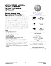
LM258, LM358, LM358A, LM2904, LM2904A, LM2904V, NCV2904, NCV2904V
www.onsemi.com
4
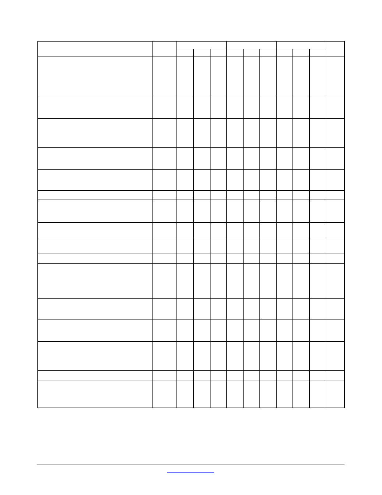
ELECTRICAL CHARACTERISTICS (V
CC
= 5.0 V, V
EE
= GND, T
A
= 25°C, unless otherwise noted.)
Characteristic
Symbo
l
LM258 LM358 LM358A
Unit
Min Typ Max Min Typ Max Min Typ Max
Input Offset Voltage
V
CC
= 5.0 V to 30 V, V
IC
= 0 V to V
CC
−1.7 V,
V
O
] 1.4 V, R
S
= 0
V
IO
mV
T
A
= 25°C − 2.0 5.0 − 2.0 7.0 − 2.0 3.0
T
A
= T
high
(Note 4) − − 7.0 − − 9.0 − − 5.0
T
A
= T
low
(Note 4) − − 7.0 − − 9.0 − − 5.0
Average Temperature Coefficient of Input Offset
Voltage
V
IO
/T
− 7.0 − − 7.0 − − 7.0 −
V/°C
T
A
= T
high
to T
low
(Note 4)
Input Offset Current I
IO
− 3.0 30 − 5.0 50 − 5.0 30 nA
T
A
= T
high
to T
low
(Note 4) − − 100 − − 150 − − 75
Input Bias Current I
IB
− −45 −150 − −45 −250 − −45 −100
T
A
= T
high
to T
low
(Note 4) − −50 −300 − −50 −500 − −50 −200
Average Temperature Coefficient of Input Offset
Current
I
IO
/T
− 10 − − 10 − − 10 − pA/°C
T
A
= T
high
to T
low
(Note 4)
Input Common Mode Voltage Range (Note 5),
V
CC
= 30 V
V
ICR
0 − 28.3 0 − 28.3 0 − 28.5 V
V
CC
= 30 V, T
A
= T
high
to T
low
0 − 28 0 − 28 0 − 28
Differential Input Voltage Range V
IDR
− − V
CC
− − V
CC
− − V
CC
V
Large Signal Open Loop Voltage Gain A
VOL
V/mV
R
L
= 2.0 k, V
CC
= 15 V, For Large V
O
Swing,
50 100 − 25 100 − 25 100 −
T
A
= T
high
to T
low
(Note 4) 25 − − 15 − − 15 − −
Channel Separation CS − −120 − − −120 − − −120 − dB
1.0 kHz ≤ f ≤ 20 kHz, Input Referenced
Common Mode Rejection
CMR 70 85 − 65 70 − 65 70 − dB
R
S
≤ 10 k
Power Supply Rejection PSR 65 100 − 65 100 − 65 100 − dB
Output Voltage−High Limit
T
A
= T
high
to T
low
(Note 4)
V
OH
V
V
CC
= 5.0 V, R
L
= 2.0 k, T
A
= 25°C
3.3 3.5 − 3.3 3.5 − 3.3 3.5 −
V
CC
= 30 V, R
L
= 2.0 k
26 − − 26 − − 26 − −
V
CC
= 30 V, R
L
= 10 k
27 28 − 27 28 − 27 28 −
Output Voltage−Low Limit V
OL
− 5.0 20 − 5.0 20 − 5.0 20 mV
V
CC
= 5.0 V, R
L
= 10 k,
T
A
= T
high
to T
low
(Note 4)
Output Source Current I
O+
mA
V
ID
= +1.0 V, V
CC
= 15 V 20 40 − 20 40 − 20 40 −
T
A
= T
high
to T
low
(LM358A Only) 10 − −
Output Sink Current I
O−
V
ID
= −1.0 V, V
CC
= 15 V 10 20 − 10 20 − 10 20 − mA
T
A
= T
high
to T
low
(LM358A Only) 5.0 − − mA
V
ID
= −1.0 V, V
O
= 200 mV 12 50 − 12 50 − 12 50 −
A
Output Short Circuit to Ground (Note 6) I
SC
− 40 60 − 40 60 − 40 60 mA
Power Supply Current (Total Device)
T
A
= T
high
to T
low
(Note 4)
I
CC
mA
V
CC
= 30 V, V
O
= 0 V, R
L
= ∞ − 1.5 3.0 − 1.5 3.0 − 1.5 2.0
V
CC
= 5 V, V
O
= 0 V, R
L
= ∞ − 0.7 1.2 − 0.7 1.2 − 0.7 1.2
4. LM258: T
low
= −25°C, T
high
= +85°C LM358, LM358A: T
low
= 0°C, T
high
= +70°C
LM2904/LM2904A: T
low
= −40°C, T
high
= +105°C LM2904V & NCV2904: T
low
= −40°C, T
high
= +125°C
NCV2904 and NCV2904V are qualified for automotive use. NCV2904V: T
low
= −40°C, T
high
= +150°C
5. The input common mode voltage or either input signal voltage should not be allowed to go negative by more than 0.3 V. The upper end of
the common mode voltage range is V
CC
− 1.7 V.
6. Short circuits from the output to V
CC
can cause excessive heating and eventual destruction. Destructive dissipation can result from
simultaneous shorts on all amplifiers.
器件 Datasheet 文档搜索
AiEMA 数据库涵盖高达 72,405,303 个元件的数据手册,每天更新 5,000 多个 PDF 文件
