Datasheet 搜索 > 微控制器 > TI(德州仪器) > LM3S6965-IQC50-A2T 数据手册 > LM3S6965-IQC50-A2T 数据手册 476/761 页
 器件3D模型
¥ 249.791
LM3S6965-IQC50-A2T 数据手册 - TI(德州仪器)
制造商:
TI(德州仪器)
分类:
微控制器
封装:
LQFP-100
描述:
的Stellaris LM3S6965微控制器 Stellaris LM3S6965 Microcontroller
Pictures:
3D模型
符号图
焊盘图
引脚图
产品图
页面导航:
引脚图在P160P172P336P396P433P476P514P551P599P612P650Hot
典型应用电路图在P47P610
原理图在P44P45P54P55P56P160P240P260P293P335P372P395
封装尺寸在P52P749P750P752P753P754P756P757P759P760
型号编码规则在P747
标记信息在P747P757P758
封装信息在P747P751P752P756P757P758P759P760
功能描述在P95P161P172P241P260P292P336P372P397P434P476P515
技术参数、封装参数在P699P701P702P703P705
应用领域在P44P58P179P761
电气规格在P52P700P702P704P706P708P710P712P714P716
导航目录
LM3S6965-IQC50-A2T数据手册
Page:
of 761 Go
若手册格式错乱,请下载阅览PDF原文件
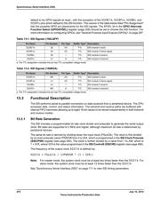
default to be GPIO signals at reset., with the exception of the SSI0Clk, SSI0Fss, SSI0Rx, and
SSI0Tx pins which default to the SSI function. The column in the table below titled "Pin Assignment"
lists the possible GPIO pin placements for the SSI signals. The AFSEL bit in the GPIO Alternate
Function Select (GPIOAFSEL) register (page 309) should be set to choose the SSI function. For
more information on configuring GPIOs, see “General-Purpose Input/Outputs (GPIOs)” on page 287.
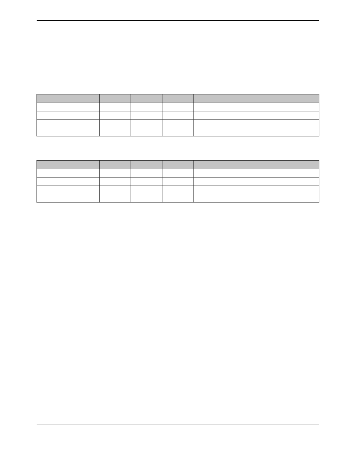
Table 13-1. SSI Signals (100LQFP)
DescriptionBuffer Type
a
Pin TypePin NumberPin Name
SSI module 0 clock.TTLI/O28SSI0Clk
SSI module 0 frame signal.TTLI/O29SSI0Fss
SSI module 0 receive.TTLI30SSI0Rx
SSI module 0 transmit.TTLO31SSI0Tx
a. The TTL designation indicates the pin has TTL-compatible voltage levels.
Table 13-2. SSI Signals (108BGA)
DescriptionBuffer Type
a
Pin TypePin NumberPin Name
SSI module 0 clock.TTLI/OM4SSI0Clk
SSI module 0 frame signal.TTLI/OL4SSI0Fss
SSI module 0 receive.TTLIL5SSI0Rx
SSI module 0 transmit.TTLOM5SSI0Tx
a. The TTL designation indicates the pin has TTL-compatible voltage levels.
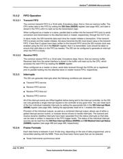
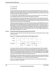
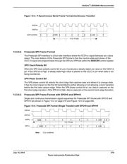
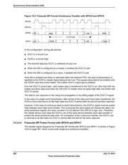
13.3 Functional Description
The SSI performs serial-to-parallel conversion on data received from a peripheral device. The CPU
accesses data, control, and status information. The transmit and receive paths are buffered with
internal FIFO memories allowing up to eight 16-bit values to be stored independently in both transmit
and receive modes.
13.3.1 Bit Rate Generation
The SSI includes a programmable bit rate clock divider and prescaler to generate the serial output
clock. Bit rates are supported to 2 MHz and higher, although maximum bit rate is determined by
peripheral devices.
The serial bit rate is derived by dividing down the input clock (FSysClk). The clock is first divided
by an even prescale value CPSDVSR from 2 to 254, which is programmed in the SSI Clock Prescale
(SSICPSR) register (see page 495). The clock is further divided by a value from 1 to 256, which is
1 + SCR, where SCR is the value programmed in the SSI Control0 (SSICR0) register (see page 488).
The frequency of the output clock SSIClk is defined by:
SSIClk = FSysClk / (CPSDVSR * (1 + SCR))
Note: For master mode, the system clock must be at least two times faster than the SSIClk. For
slave mode, the system clock must be at least 12 times faster than the SSIClk.
See “Synchronous Serial Interface (SSI)” on page 711 to view SSI timing parameters.
July 15, 2014476
Texas Instruments-Production Data
Synchronous Serial Interface (SSI)
器件 Datasheet 文档搜索
AiEMA 数据库涵盖高达 72,405,303 个元件的数据手册,每天更新 5,000 多个 PDF 文件
