Datasheet 搜索 > DC/DC转换器 > TI(德州仪器) > LM43603PWP 数据手册 > LM43603PWP 数据手册 19/52 页
 器件3D模型
¥ 11.091
LM43603PWP 数据手册 - TI(德州仪器)
制造商:
TI(德州仪器)
分类:
DC/DC转换器
封装:
HTSSOP-16
描述:
直流-直流开关同步降压稳压器, 可调, 3.5V-36V输入, 1V-28V/3A输出, HTSSOP-16
Pictures:
3D模型
符号图
焊盘图
引脚图
产品图
页面导航:
引脚图在P3Hot
典型应用电路图在P24P25P26
原理图在P1P14P15P20P22P24P25P29
封装尺寸在P45P47P48P49
焊盘布局在P42P50
标记信息在P45
封装信息在P44P45P46P47P48
技术参数、封装参数在P4
应用领域在P1P24P25P26
电气规格在P4P5P6
导航目录
LM43603PWP数据手册
Page:
of 52 Go
若手册格式错乱,请下载阅览PDF原文件
SYNC
R
TERM
EXT CLOCK
0
50
100
150
200
250
0 500 1000 1500 2000 2500
RT Resistance (kŸ)
Switching Frequency (kHz)
C008
19
LM43603
www.ti.com
SNVSA09C –APRIL 2014–REVISED FEBRUARY 2017
Product Folder Links: LM43603
Submit Documentation FeedbackCopyright © 2014–2017, Texas Instruments Incorporated
Feature Description (continued)
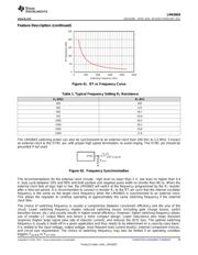
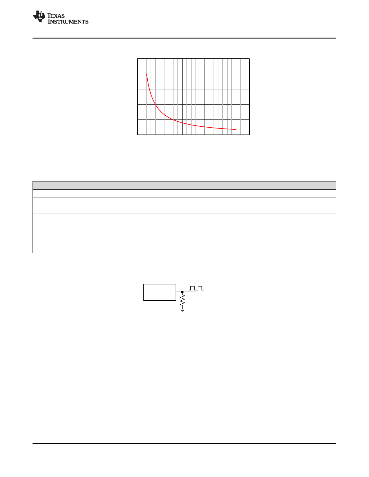
Figure 41. RT vs Frequency Curve
Table 1. Typical Frequency Setting R
T
Resistance
F
S
(kHz) R
T
(kΩ)
200 200
350 115
500 78.7
750 53.6
1000 39.2
1500 26.1
2000 19.6
2200 17.8
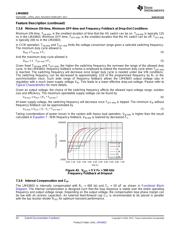
The LM43603 switching action can also be synchronized to an external clock from 200 kHz to 2.2 MHz. Connect
an external clock to the SYNC pin, with proper high speed termination, to avoid ringing. The SYNC pin should be
grounded if not used.
Figure 42. Frequency Synchronization
The recommendations for the external clock include : high level no lower than 2 V, low level no higher than 0.4
V, duty cycle between 10% and 90% and both positive and negative pulse width no shorter than 80 ns. When the
external clock fails at logic high or low, the LM43603 will switch at the frequency programmed by the R
T
resistor
after a time-out period. It is recommended to connect a resistor R
T
to the RT pin such that the internal oscillator
frequency is the same as the target clock frequency when the LM43603 is synchronized to an external clock.
This allows the regulator to continue operating at approximately the same switching frequency if the external
clock fails.
The choice of switching frequency is usually a compromise between conversion efficiency and the size of the
circuit. Lower switching frequency implies reduced switching losses (including gate charge losses, switch
transition losses, etc.) and usually results in higher overall efficiency. However, higher switching frequency allows
use of smaller LC output filters and hence a more compact design. Lower inductance also helps transient
response (higher large signal slew rate of inductor current), and reduces the DCR loss. The optimal switching
frequency is usually a trade-off in a given application and thus needs to be determined on a case-by-case basis.
It is related to the input voltage, output voltage, most frequent load current level(s), external component choices,
and circuit size requirement. The choice of switching frequency may also be limited if an operating condition
triggers T
ON-MIN
or T
OFF-MIN
.
器件 Datasheet 文档搜索
AiEMA 数据库涵盖高达 72,405,303 个元件的数据手册,每天更新 5,000 多个 PDF 文件
