Datasheet 搜索 > TI(德州仪器) > LM46002 数据手册 > LM46002 数据手册 15/51 页

¥ 0
LM46002 数据手册 - TI(德州仪器)
制造商:
TI(德州仪器)
描述:
LM46002 3.5 – 60V 2A 低静态电流降压转换器
Pictures:
3D模型
符号图
焊盘图
引脚图
产品图
页面导航:
引脚图在P3Hot
典型应用电路图在P24P25P26P27
原理图在P14P15P21P22P24P25P30
封装尺寸在P1P47P49P50
标记信息在P47
封装信息在P47P48P49P50
技术参数、封装参数在P4
应用领域在P24P25P26P27
电气规格在P4P5P6
导航目录
LM46002数据手册
Page:
of 51 Go
若手册格式错乱,请下载阅览PDF原文件
0
0
V
IN
-V
D1
t
ON
t
t
Inductor Current
D = t
ON
/ T
SW
V
SW
t
OFF
T
SW
i
L
SW Voltage
ûi
L
I
OUT
I
LPK
15
LM46002
www.ti.com.cn
ZHCSCD8B –APRIL 2014–REVISED SEPTEMBER 2014
Copyright © 2014, Texas Instruments Incorporated
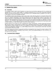
8.3 Feature Description
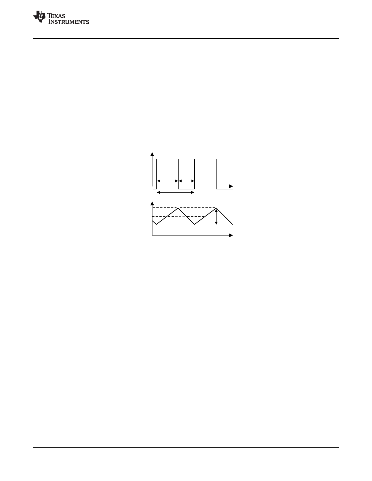
8.3.1 Fixed Frequency Peak Current Mode Controlled Step-Down Regulator
The following operating description of the LM46002 will refer to the Functional Block Diagram and to the
waveforms in Figure 33. The LM46002 is a step-down Buck regulator with both high-side (HS) switch and low-
side (LS) switch (synchronous rectifier) integrated. The LM46002 supplies a regulated output voltage by turning
on the HS and LS NMOS switches with controlled ON time. During the HS switch ON time, the SW pin voltage
V
SW
swings up to approximately V
IN
, and the inductor current I
L
increases with a linear slope (V
IN
- V
OUT
) / L.
When the HS switch is turned off by the control logic, the LS switch is turned on after a anti-shoot-through dead
time. Inductor current discharges through the LS switch with a slope of -V
OUT
/ L. The control parameter of Buck
converters are defined as Duty Cycle D = t
ON
/ T
SW
, where t
ON
is the HS switch ON time and T
SW
is the switching
period. The regulator control loop maintains a constant output voltage by adjusting the duty cycle D. In an ideal
Buck converter, where losses are ignored, D is proportional to the output voltage and inversely proportional to
the input voltage: D = V
OUT
/ V
IN
.
Figure 33. SW Node and Inductor Current Waveforms in Continuous Conduction Mode (CCM)
The LM46002 synchronous Buck converter employs peak current mode control topology. A voltage feedback
loop is used to get accurate DC voltage regulation by adjusting the peak current command based on voltage
offset. The peak inductor current is sensed from the HS switch and compared to the peak current to control the
ON time of the HS switch. The voltage feedback loop is internally compensated, which allows for fewer external
components, makes it easy to design, and provides stable operation with almost any combination of output
capacitors. The regulator operates with fixed switching frequency in Continuous Conduction Mode (CCM) and
Discontinuous Conduction Mode (DCM). At very light load, the LM46002 will operate in PFM to maintain high
efficiency and the switching frequency will decrease with reduced load current.
8.3.2 Light Load Operation
DCM operation is employed in the LM46002 when the inductor current valley reaches zero. The LM46002 will be
in DCM when load current is less than half of the peak-to-peak inductor current ripple in CCM. In DCM, the LS
switch is turned off when the inductor current reaches zero. Switching loss is reduced by turning off the LS FET
at zero current and the conduction loss is lowered by not allowing negative current conduction. Power conversion
efficiency is higher in DCM than CCM under the same conditions.
In DCM, the HS switch ON time will reduce with lower load current. When either the minimum HS switch ON time
(T
ON-MIN
) or the minimum peak inductor current (I
PEAK-MIN
) is reached, the switching frequency will decrease to
maintain regulation. At this point, the LM46002 operates in PFM. In PFM, switching frequency is decreased by
the control loop when load current reduces to maintain output voltage regulation. Switching loss is further
reduced in PFM operation due to less frequent switching actions. Figure 34 shows an example of switching
frequency decreases with decreased load current.
器件 Datasheet 文档搜索
AiEMA 数据库涵盖高达 72,405,303 个元件的数据手册,每天更新 5,000 多个 PDF 文件
