Datasheet 搜索 > DC/DC转换器 > TI(德州仪器) > LM5017MRX/NOPB 数据手册 > LM5017MRX/NOPB 数据手册 2/31 页


¥ 5.78
LM5017MRX/NOPB 数据手册 - TI(德州仪器)
制造商:
TI(德州仪器)
分类:
DC/DC转换器
封装:
PowerSOIC-8
描述:
100V输入,600mA恒准时同步降压转换器
Pictures:
3D模型
符号图
焊盘图
引脚图
产品图
页面导航:
引脚图在P3Hot
典型应用电路图在P1P14
原理图在P8P14P18
封装尺寸在P25P27P28
标记信息在P25
封装信息在P24P25P26P27P28
技术参数、封装参数在P4P14P24
应用领域在P1P31
电气规格在P4P5P14P15
导航目录
LM5017MRX/NOPB数据手册
Page:
of 31 Go
若手册格式错乱,请下载阅览PDF原文件

LM5017
SNVS783H –JANUARY 2012–REVISED DECEMBER 2014
www.ti.com
Table of Contents
7.3 Feature Description................................................... 9
1 Features.................................................................. 1
7.4 Device Functional Modes ....................................... 13
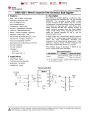
2 Applications ........................................................... 1
8 Application and Implementation ........................ 14
3 Description............................................................. 1
8.1 Application Information............................................ 14
4 Revision History..................................................... 2
8.2 Typical Application ................................................. 14
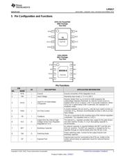
5 Pin Configuration and Functions......................... 3
9 Power Supply Recommendations...................... 23
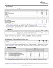
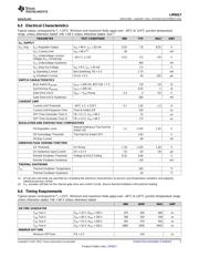
6 Specifications......................................................... 4
10 Layout................................................................... 23
6.1 Absolute Maximum Ratings ..................................... 4
10.1 Layout Guidelines ................................................. 23
6.2 ESD Ratings.............................................................. 4
10.2 Layout Example .................................................... 23
6.3 Recommended Operating Conditions....................... 4
11 Device and Documentation Support ................. 24
6.4 Thermal Information ................................................. 4
11.1 Documentation Support ........................................ 24
6.5 Electrical Characteristics........................................... 5
11.2 Trademarks........................................................... 24
6.6 Timing Requirements................................................ 5
11.3 Electrostatic Discharge Caution............................ 24
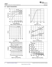
6.7 Typical Characteristics.............................................. 6
11.4 Glossary................................................................ 24
7 Detailed Description.............................................. 8
12 Mechanical, Packaging, and Orderable
7.1 Overview................................................................... 8
Information........................................................... 24
7.2 Functional Block Diagram......................................... 8
4 Revision History
Changes from Revision G (December 2013) to Revision H Page
• Added package designators to pin out drawings. ................................................................................................................. 3
• Changed Thermal Information table. ..................................................................................................................................... 4
• Added D1 to Figure 12 ......................................................................................................................................................... 13
• Updated the calculation for K from 10
-10
to 10
-11
.................................................................................................................. 15
• Changed Series Ripple Resistor R
C
section to Type III Ripple Circuit ................................................................................ 16
Changes from Revision F (September 2013) to Revision G Page
• Changed formatting throughout document to the TI standard ............................................................................................... 1
• Changed minimum operating input voltage from 9 V to 7.5 V in Features ........................................................................... 1
• Changed minimum operating input voltage from 9 V to 7.5 V in Typical Application ........................................................... 1
• Changed minimum operating input voltage from 9 V to 7.5 V in Pin Descriptions ............................................................... 3
• Added Maximum Junction Temperature................................................................................................................................. 4
• Changed minimum operating input voltage from 9 V to 7.5 V in Recommended Operating Conditions .............................. 4
Changes from Revision E (July 2013) to Revision F Page
• Added SW to RTN (100 ns transient) to Absolute Maximum Ratings ................................................................................... 4
2 Submit Documentation Feedback Copyright © 2012–2014, Texas Instruments Incorporated
Product Folder Links: LM5017
器件 Datasheet 文档搜索
AiEMA 数据库涵盖高达 72,405,303 个元件的数据手册,每天更新 5,000 多个 PDF 文件
