Datasheet 搜索 > 负载控制器 > TI(德州仪器) > LM5069MM-1/NOPB 数据手册 > LM5069MM-1/NOPB 数据手册 10/28 页
 器件3D模型
¥ 10.065
LM5069MM-1/NOPB 数据手册 - TI(德州仪器)
制造商:
TI(德州仪器)
分类:
负载控制器
封装:
VSSOP-10
描述:
TEXAS INSTRUMENTS LM5069MM-1/NOPB 芯片, 热插拔控制器, 48V
Pictures:
3D模型
符号图
焊盘图
引脚图
产品图
页面导航:
引脚图在P2Hot
典型应用电路图在P1
原理图在P9P10
封装尺寸在P23P25P26
标记信息在P23
封装信息在P23P24P25P26
功能描述在P10
技术参数、封装参数在P3
应用领域在P1P2P13P14P28
电气规格在P3P4P5P6P7P8

导航目录
LM5069MM-1/NOPB数据手册
Page:
of 28 Go
若手册格式错乱,请下载阅览PDF原文件
LOAD
VIN
GND
GND
BACKPLANE
PLUG- IN BOARD
V
SYS
PGD
OUT
R
S
Q1
C
L
LIVE
V
OUT
LM5069
+48V
LM5069
Power
Good
UVLO
OVLO
PWR
GNDTIMER
PGD
OUT
SENSE GATE
R1
Q1
R
S
C
IN
V
SYS
R2
R3
R
PG
V
OUT
R
PWR
C
L
C
T
LM5069
SNVS452D –SEPTEMBER 2006–REVISED MAY 2013
www.ti.com
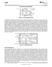
FUNCTIONAL DESCRIPTION
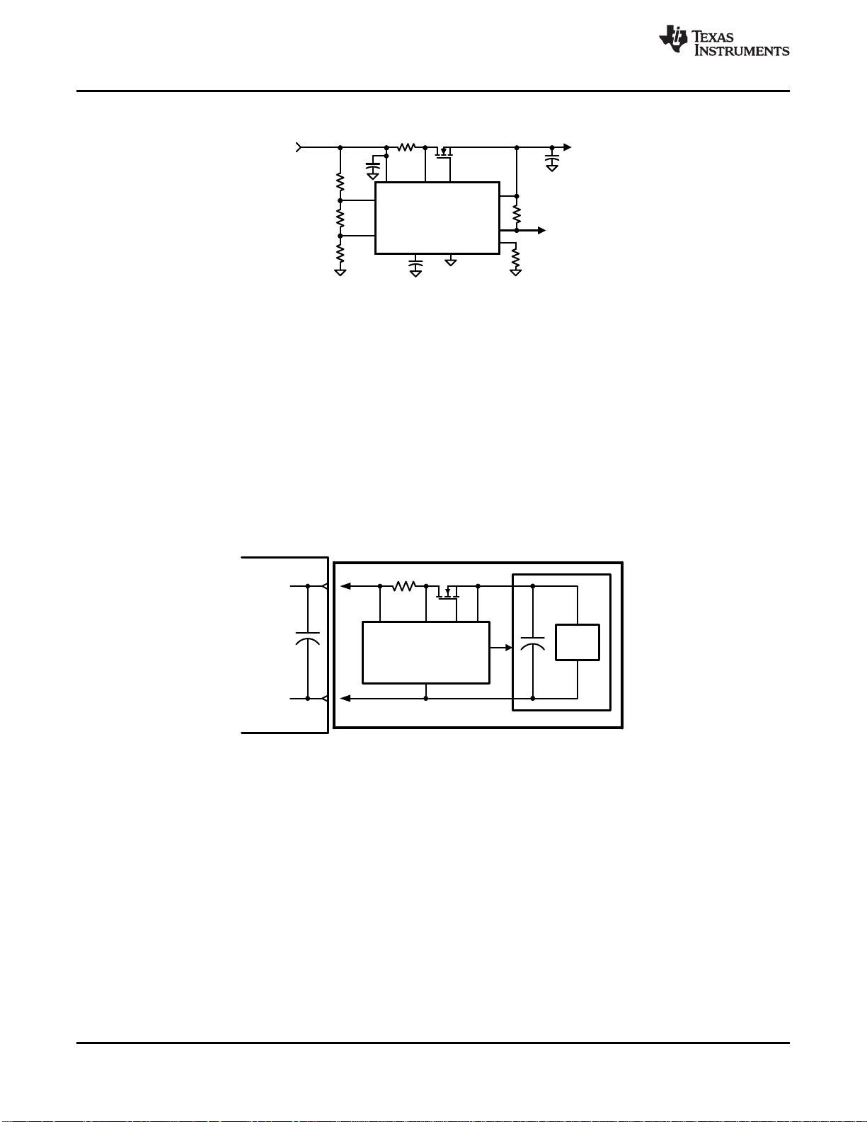
Figure 22. Basic Application Circuit
The LM5069 is designed to control the in-rush current to the load upon insertion of a circuit card into a live
backplane or other "hot" power source, thereby limiting the voltage sag on the backplane’s supply voltage, and
the dV/dt of the voltage applied to the load. Effects on other circuits in the system are minimized, preventing
possible unintended resets. A controlled shutdown when the circuit card is removed can also be implemented
using the LM5069. In addition to a programmable current limit, the LM5069 monitors and limits the maximum
power dissipation in the series pass device to maintain operation within the device Safe Operating Area (SOA).
Either current limiting or power limiting for an extended period of time results in the shutdown of the series pass
device. In this event, the LM5069-1 latches off until the circuit is re-enabled by external control, while the
LM5069-2 automatically restarts with defined timing. The circuit breaker function quickly switches off the series
pass device upon detection of a severe over-current condition. The Power Good (PGD) output pin indicates
when the output voltage is within 1.25V of the system input voltage (V
SYS
). Programmable under-voltage lock-out
(UVLO) and over-voltage lock-out (OVLO) circuits shut down the LM5069 when the system input voltage is
outside the desired operating range. The typical configuration of a circuit card with LM5069 hot swap protection
is shown in Figure 23.
Figure 23. LM5069 Application
Power Up Sequence
The VIN operating range of the LM5069 is +9V to +80V, with a transient capability to +100V. Referring to the
Block Diagram and Figure 22 and Figure 24, as the voltage at VIN initially increases, the external N-channel
MOSFET (Q1) is held off by an internal 230 mA pull-down current at the GATE pin. The strong pull-down current
at the GATE pin prevents an inadvertent turn-on as the MOSFET’s gate-to-drain (Miller) capacitance is charged.
Additionally, the TIMER pin is initially held at ground. When the VIN voltage reaches the POR
IT
threshold (7.6V)
the insertion time begins. During the insertion time, the capacitor at the TIMER pin (C
T
) is charged by a 5.5 µA
current source, and Q1 is held off by a 2 mA pull-down current at the GATE pin regardless of the VIN voltage.
The insertion time delay allows ringing and transients at VIN to settle before Q1 can be enabled. The insertion
time ends when the TIMER pin voltage reaches 4.0V. C
T
is then quickly discharged by an internal 1.5 mA pull-
down current. After the insertion time, the LM5069 control circuitry is enabled when VIN reaches the POR
EN
threshold (8.4V). The GATE pin then switches on Q1 when V
SYS
exceeds the UVLO threshold (UVLO pin >2.5V).
If V
SYS
is above the UVLO threshold at the end of the insertion time, Q1 switches on at that time. The GATE pin
charge pump sources 16 µA to charge Q1’s gate capacitance. The maximum gate-to-source voltage of Q1 is
limited by an internal 12V zener diode.
10 Submit Documentation Feedback Copyright © 2006–2013, Texas Instruments Incorporated
Product Folder Links: LM5069
器件 Datasheet 文档搜索
AiEMA 数据库涵盖高达 72,405,303 个元件的数据手册,每天更新 5,000 多个 PDF 文件
