Datasheet 搜索 > FET驱动器 > TI(德州仪器) > LM5100AMRX/NOPB 数据手册 > LM5100AMRX/NOPB 数据手册 6/36 页
 器件3D模型
¥ 19.387
LM5100AMRX/NOPB 数据手册 - TI(德州仪器)
制造商:
TI(德州仪器)
分类:
FET驱动器
封装:
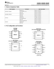
HSOP-8
描述:
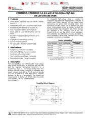
3A , 2A和1A高电压高侧和低侧栅极驱动器 3A, 2A and 1A High Voltage High-Side and Low-Side Gate Drivers
Pictures:
3D模型
符号图
焊盘图
引脚图
产品图
页面导航:
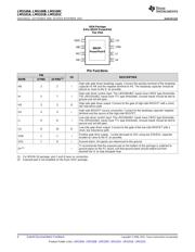
引脚图在P3P4Hot
典型应用电路图在P16P17
原理图在P1P14
封装尺寸在P23P24P26P27P28
焊盘布局在P21
标记信息在P23P24P25
封装信息在P22P23P24P25P26P27P28
技术参数、封装参数在P5
应用领域在P1
电气规格在P6P7
导航目录
LM5100AMRX/NOPB数据手册
Page:
of 36 Go
若手册格式错乱,请下载阅览PDF原文件
LM5100A
,
LM5100B
,
LM5100C
LM5101A
,
LM5101B
,
LM5101C
SNOSAW2Q –SEPTEMBER 2006–REVISED NOVEMBER 2015
www.ti.com
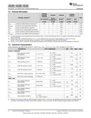
7.4 Thermal Information
LM5100A,
LM5100x,
LM5100C, LM5101C LM5101A
LM5101x
LM5101A
THERMAL METRIC
(1)
UNIT
MSOP-
SO PowerPAD WSON
(2)
WSON
(2)
SOIC
PowerPAD
(2)
8 PINS 8 PINS 8 PINS 10 PINS 8 PINS
R
θJA
Junction-to-ambient thermal resistance
(3)
40 80 37.8 40 170 °C/W
R
θJC(top)
Junction-to-case (top) thermal resistance — — 36.7 — — °C/W
R
θJB
Junction-to-board thermal resistance — — 14.9 — — °C/W
ψ
JT
Junction-to-top characterization parameter — — 0.3 — — °C/W
ψ
JB
Junction-to-board characterization parameter — — 15.2 — — °C/W
R
θJC(bot)
Junction-to-case (bottom) thermal resistance — — 4.4 — — °C/W
(1) For more information about traditional and new thermal metrics, see the Semiconductor and IC Package Thermal Metrics application
report, SPRA953.
(2) 4-layer board with Cu finished thickness 1.5, 1, 1, 1.5 oz. Maximum die size used. 5× body length of Cu trace on PCB top.
50-mm × 50-mm ground and power planes embedded in PCB. See Application Note AN-1187 (SNOA401).
(3) The R
θJA
is not a given constant for the package and depends on the printed circuit board design and the operating environment.
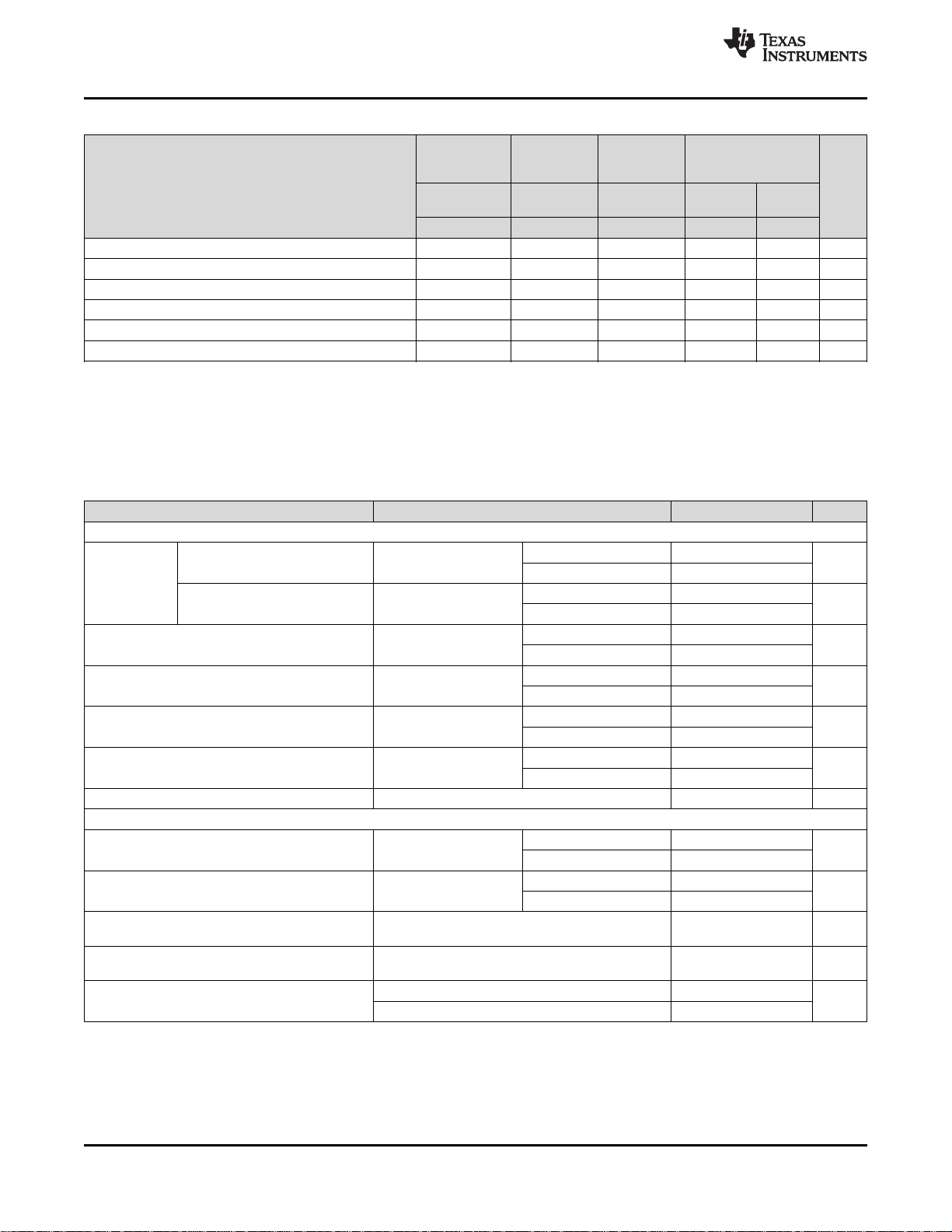
7.5 Electrical Characteristics
unless otherwise specified, limits are for T
J
= 25°C, V
DD
= V
HB
= 12 V, V
SS
= V
HS
= 0 V, no load on LO or HO
(1)
.
PARAMETER TEST CONDITIONS MIN TYP MAX UNIT
SUPPLY CURRENTS
T
J
= 25°C 0.1
VDD quiescent current,
LI = HI = 0 V mA
LM5100A/B/C
T
J
= –40°C to 125°C 0.2
I
DD
T
J
= 25°C 0.25
VDD quiescent current,
LI = HI = 0 V mA
LM5101A/B/C
T
J
= –40°C to 125°C 0.4
T
J
= 25°C 2
I
DDO
VDD operating current f = 500 kHz mA
T
J
= –40°C to 125°C 3
T
J
= 25°C 0.06
I
HB
Total HB quiescent current LI = HI = 0 V mA
T
J
= –40°C to 125°C 0.2
T
J
= 25°C 1.6
I
HBO
Total HB operating current f = 500 kHz mA
T
J
= –40°C to 125°C 3
T
J
= 25°C 0.1
I
HBS
HB to VSS current, quiescent HS = HB = 100 V µA
T
J
= –40°C to 125°C 10
I
HBSO
HB to VSS current, operating f = 500 kHz 0.4 mA
INPUT PINS
T
J
= 25°C 5.4
Input voltage threshold
V
IL
Rising Edge V
LM5100A/B/C
T
J
= –40°C to 125°C 4.5 6.3
T
J
= 25°C 1.8
Input voltage threshold
V
IL
Rising Edge V
LM5101A/B/C
T
J
= –40°C to 125°C 1.3 2.3
Input voltage hysteresis
V
IHYS
500 mV
LM5100A/B/C
Input voltage hysteresis
V
IHYS
50 mV
LM5101A/B/C
T
J
= 25°C 200
R
I
Input pulldown resistance kΩ
T
J
= –40°C to 125°C 100 400
(1) Minimum and maximum limits are 100% production tested at 25°C. Limits over the operating temperature range are specified through
correlation using Statistical Quality Control (SQC) methods. Limits are used to calculate Average Outgoing Quality Level (AOQL).
6 Submit Documentation Feedback Copyright © 2006–2015, Texas Instruments Incorporated
Product Folder Links: LM5100A LM5100B LM5100C LM5101A LM5101B LM5101C
器件 Datasheet 文档搜索
AiEMA 数据库涵盖高达 72,405,303 个元件的数据手册,每天更新 5,000 多个 PDF 文件
