Datasheet 搜索 > 稳压芯片 > TI(德州仪器) > LM5117PSQE/NOPB 数据手册 > LM5117PSQE/NOPB 数据手册 4/43 页

¥ 25.125
LM5117PSQE/NOPB 数据手册 - TI(德州仪器)
制造商:
TI(德州仪器)
分类:
稳压芯片
封装:
WQFN-24
描述:
具有模拟电流监视器的 5.5-65V 宽输入电压、电流模式同步降压控制器 24-WQFN -40 to 125
Pictures:
3D模型
符号图
焊盘图
引脚图
产品图
页面导航:
引脚图在P3P4P5Hot
典型应用电路图在P1P22
原理图在P11P12P22
封装尺寸在P37P39P40
焊盘布局在P35
标记信息在P37P38
封装信息在P36P37P38P39P40
技术参数、封装参数在P5
应用领域在P1P22P43
电气规格在P6P7P8
导航目录
LM5117PSQE/NOPB数据手册
Page:
of 43 Go
若手册格式错乱,请下载阅览PDF原文件
LM5117
,
LM5117-Q1
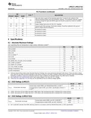
SNVS698F –APRIL 2011–REVISED AUGUST 2015
www.ti.com
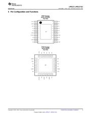
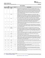
Pin Functions
PIN
TYPE
(1)
DESCRIPTION
HTSSOP WQFN NAME
1 24 UVLO Undervoltage lockout programming pin. If the UVLO pin voltage is below 0.4 V, the
regulator is in the shutdown mode with all functions disabled. If the UVLO pin voltage is
greater than 0.4 V and less than 1.25 V, the regulator is in standby mode with the VCC
regulator operational, the SS pin grounded, and no switching at the HO and LO outputs.
I
If the UVLO pin voltage is above 1.25 V, the SS pin is allowed to ramp and pulse width
modulated gate drive signals are delivered to the HO and LO pins. A 20μA current
source is enabled when UVLO exceeds 1.25 V and flows through the external UVLO
resistors to provide hysteresis.
2 1 DEMB Optional logic input that enables diode emulation when in the low state. In diode
emulation mode, the low-side NMOS is latched off for the remainder of the PWM cycle
after detecting reverse current flow (current flow from output to ground through the low-
I
side NMOS). When DEMB is high, diode emulation is disabled allowing current to flow in
either direction through the low-side NMOS. A 50-kΩ pull-down resistor internal to the
LM5117 holds DEMB pin low and enables diode emulation if the pin is left floating.
3 2 RES The restart timer pin that configures the hiccup mode current limiting. A capacitor on the
RES pin determines the time the controller remains off before automatically restarting.
O The hiccup mode commences when the controller experiences 256 consecutive PWM
cycles of cycle-by-cycle current limiting. After this occurs, a 10-μA current source
charges the RES pin capacitor to the 1.25 V threshold and restarts LM5117.
4 3 SS An external capacitor and an internal 10-μA current source set the ramp rate of the error
I amplifier reference during soft-start. The SS pin is held low when VCC< 5 V, UVLO <
1.25 V or during thermal shutdown.
5 4 RT The internal oscillator is programmed with a single resistor between RT and the AGND.
The recommended maximum oscillator frequency is 750kHz. The internal oscillator can
I
be synchronized to an external clock by coupling a positive pulse into the RT pin through
a small coupling capacitor.
6 5 AGND G Analog ground. Return for the internal 0.8 V voltage reference and analog circuits.
7 7 VCCDIS Optional input that disables the internal VCC regulator. If VCCDIS>1.25 V, the internal
VCC regulator is disabled. VCCDIS has an internal 500-kΩ pulldown resistor to enable
I the VCC regulator when the pin is left floating. The internal 500-kΩ pull-down resistor can
be overridden by pulling VCCDIS above 1.25 V with a resistor divider connected to an
external bias supply.
8 8 FB Feedback. Inverting input of the internal error amplifier. A resistor divider from the output
I
to this pin sets the output voltage level. The regulation threshold at the FB pin is 0.8 V.
9 9 COMP Output of the internal error amplifier. The loop compensation network should be
O
connected between this pin and the FB pin.
10 10 CM Current monitor output. Average of the sensed inductor current is provided. Monitor
O
directly between CM and AGND. CM should be left floating when the pin is not used.
11 11 RAMP PWM ramp signal. An external resistor and capacitor connected between the SW pin, the
RAMP pin and the AGND pin sets the PWM ramp slope. Proper selection of component
I
values produces a RAMP signal that emulates the AC component of the inductor with a
slope proportional to input supply voltage.
12 12 CS I Current sense amplifier input. Connect to the high-side of the current sense resistor.
13 13 CSG Kelvin ground connection to the current sense resistor. Connect directly to the low-side of
G
the current sense resistor.
14 14 PGND Power ground return pin for low-side NMOS gate driver. Connect directly to the low-side
O
of the current sense resistor.
15 15 LO Low-side NMOS gate drive output. Connect to the gate of the low-side synchronous
P/O/I
NMOS transistor through a short, low inductance path.
16 16 VCC Bias supply pin. Locally decouple to PGND using a low ESR/ESL capacitor located as
I/O
close to controller as possible.
17 18 SW Switching node of the buck regulator. Connect to the bootstrap capacitor, the source
O terminal of the high-side NMOS transistor and the drain terminal of the low-side NMOS
through a short, low inductance path.
18 19 HO High-side NMOS gate drive output. Connect to the gate of the high-side NMOS transistor
P
through a short, low inductance path.
(1) I = Input, O = Output, G = Ground, P = Power
4 Submit Documentation Feedback Copyright © 2011–2015, Texas Instruments Incorporated
Product Folder Links: LM5117 LM5117-Q1
器件 Datasheet 文档搜索
AiEMA 数据库涵盖高达 72,405,303 个元件的数据手册,每天更新 5,000 多个 PDF 文件
