Datasheet 搜索 > 运算放大器 > TI(德州仪器) > LM6172AMGWRLQV 数据手册 > LM6172AMGWRLQV 数据手册 14/25 页

¥ 4187.621
LM6172AMGWRLQV 数据手册 - TI(德州仪器)
制造商:
TI(德州仪器)
分类:
运算放大器
封装:
CFP-16
描述:
双高速,低功耗,低失真,电压反馈型放大器 Dual High Speed, Low Power, Low Distortion, Voltage Feedback Amplifiers
Pictures:
3D模型
符号图
焊盘图
引脚图
产品图
页面导航:
典型应用电路图在P18
原理图在P2P14
封装尺寸在P20P21
标记信息在P20P21P22
封装信息在P20P21P22
技术参数、封装参数在P3
应用领域在P1P22P25
电气规格在P3P4P5P6P7P8P9P10P11P12P13
导航目录
LM6172AMGWRLQV数据手册
Page:
of 25 Go
若手册格式错乱,请下载阅览PDF原文件
LM6172QML
SNOSAR4A –DECEMBER 2010–REVISED OCTOBER 2011
www.ti.com
APPLICATION NOTES
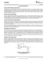
LM6172 PERFORMANCE DISCUSSION
The LM6172 is a dual high-speed, low power, voltage feedback amplifier. It is unity-gain stable and offers
outstanding performance with only 2.3mA of supply current per channel. The combination of 100MHz unity-gain
bandwidth, 3000V/μs slew rate, 50mA per channel output current and other attractive features makes it easy to
implement the LM6172 in various applications. Quiescent power of the LM6172 is 138mW operating at ±15V
supply and 46mW at ±5V supply.
LM6172 CIRCUIT OPERATION
The class AB input stage in LM6172 is fully symmetrical and has a similar slewing characteristic to the current
feedback amplifiers. In the LM6172 Simplified Schematic (Page 2), Q1 through Q4 form the equivalent of the
current feedback input buffer, R
E
the equivalent of the feedback resistor, and stage A buffers the inverting input.
The triple-buffered output stage isolates the gain stage from the load to provide low output impedance.
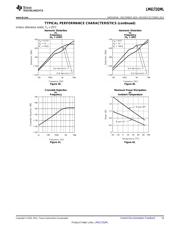
LM6172 SLEW RATE CHARACTERISTIC
The slew rate of LM6172 is determined by the current available to charge and discharge an internal high
impedance node capacitor. This current is the differential input voltage divided by the total degeneration resistor
R
E
. Therefore, the slew rate is proportional to the input voltage level, and the higher slew rates are achievable in
the lower gain configurations.
When a very fast large signal pulse is applied to the input of an amplifier, some overshoot or undershoot occurs.
By placing an external series resistor such as 1kΩ to the input of LM6172, the slew rate is reduced to help lower
the overshoot, which reduces settling time.
REDUCING SETTLING TIME
The LM6172 has a very fast slew rate that causes overshoot and undershoot. To reduce settling time on
LM6172, a 1kΩ resistor can be placed in series with the input signal to decrease slew rate. A feedback capacitor
can also be used to reduce overshoot and undershoot. This feedback capacitor serves as a zero to increase the
stability of the amplifier circuit. A 2pF feedback capacitor is recommended for initial evaluation. When the
LM6172 is configured as a buffer, a feedback resistor of 1kΩ must be added in parallel to the feedback capacitor.
Another possible source of overshoot and undershoot comes from capacitive load at the output. Please see the
section “ Driving Capacitive Loads” for more detail.
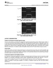
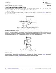
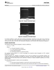
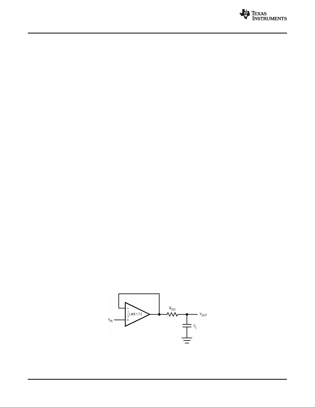
DRIVING CAPACITIVE LOADS
Amplifiers driving capacitive loads can oscillate or have ringing at the output. To eliminate oscillation or reduce
ringing, an isolation resistor can be placed as shown in Figure 43. The combination of the isolation resistor and
the load capacitor forms a pole to increase stability by adding more phase margin to the overall system. The
desired performance depends upon the value of the isolation resistor; the bigger the isolation resistor, the more
damped (slow) the pulse response becomes. For LM6172, a 50Ω isolation resistor is recommended for initial
evaluation.
Figure 43. Isolation Resistor Used
to Drive Capacitive Load
14 Submit Documentation Feedback Copyright © 2010–2011, Texas Instruments Incorporated
Product Folder Links: LM6172QML
器件 Datasheet 文档搜索
AiEMA 数据库涵盖高达 72,405,303 个元件的数据手册,每天更新 5,000 多个 PDF 文件
