Datasheet 搜索 > National Semiconductor(美国国家半导体) > LM6361 数据手册 > LM6361 数据手册 3/11 页


¥ 0
LM6361 数据手册 - National Semiconductor(美国国家半导体)
制造商:
National Semiconductor(美国国家半导体)
封装:
DIP
描述:
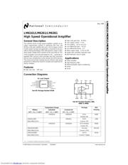
高速运算放大器 High Speed Operational Amplifier
Pictures:
3D模型
符号图
焊盘图
引脚图
产品图
LM6361数据手册
Page:
of 11 Go
若手册格式错乱,请下载阅览PDF原文件
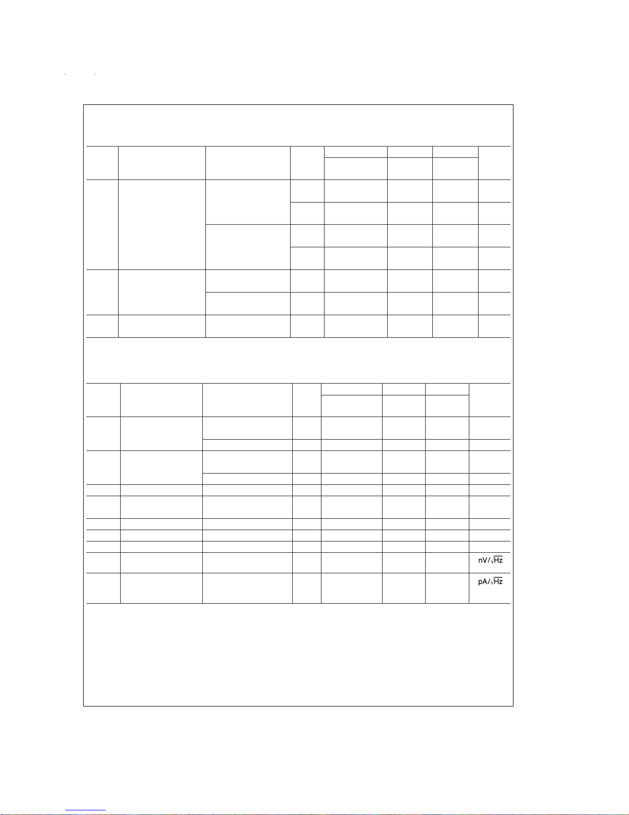
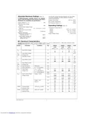
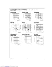
DC Electrical Characteristics (Continued)
The following specifications apply for Supply Voltage
=
±
15V, V
CM
=
0, R
L
≥ 100 kΩ and R
S
=
50Ω unless otherwise noted.
Boldface limits apply for T
J
=
T
MIN
to T
MAX
; all other limits T
J
=
25˚C.
Symbol Parameter Conditions Typ LM6161 LM6261 LM6361 Units
Limit Limit Limit
(Notes 3, 11) (Note 3) (Note 3)
V
O
Output Voltage Supply
=
±
15V +14.2 +13.5 +13.5 +13.4 Volts
Swing and R
L
=
2kΩ +13.3 +13.3 +13.3 Min
−13.4 −13.0 −13.0 −12.9 Volts
−12.7 −12.8 −12.8 Min
Supply
=
+5V 4.2 3.5 3.5 3.4 Volts
and R
L
=
2kΩ 3.3 3.3 3.3 Min
(Note 4) 1.3 1.7 1.7 1.8 Volts
2.0 1.9 1.9 Max
Output Short Source 65 30 30 30 mA
Circuit Current 20 25 25 Min
Sink 65 30 30 30 mA
20 25 25 Min
I
S
Supply Current 5.0 6.5 6.5 6.8 mA
6.8 6.7 6.9 Max
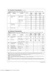
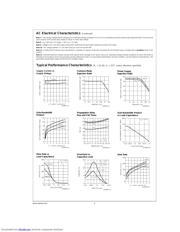
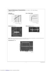
AC Electrical Characteristics
The following specifications apply for Supply Voltage
=
±
15V, V
CM
=
0, R
L
≥ 100 kΩ and R
S
=
50Ω unless otherwise noted.
Boldface limits apply for T
J
=
T
MIN
to T
MAX
; all other limits T
J
=
25˚C.
LM6161 LM6261 LM6361
Symbol Parameter Conditions Typ Limit Limit Limit Units
(Notes 3, 11) (Note 3) (Note 3)
GBW Gain-Bandwidth
@
f
=
20 MHz 50 40 40 35 MHz
Product 30 35 32 Min
Supply
=
±
5V 35 MHz
SR Slew Rate A
V
=
+1 (Note 8) 300 200 200 200 V/µs
180 180 180 Min
Supply
=
±
5V (Note 8) 200 V/µs
PBW Power Bandwidth V
OUT
=
20 V
PP
4.5 MHz
t
S
Settling Time 10V Step to 0.1
%
120 ns
A
V
=
−1, R
L
=
2kΩ
φm Phase Margin 45 Deg
A
D
Differential Gain NTSC, A
V
=
+4
<
0.1
%
φD Differential Phase NTSC, A
V
=
+4 0.1 Deg
e
np-p
Input Noise Voltage f
=
10 kHz 15
i
np-p
Input Noise Current f
=
10 kHz 1.5
Note 1: Continuous short-circuit operation at elevated ambient temperature can result in exceeding the maximum allowed junction temperature of 150˚C.
Note 2: The typical junction-to-ambient thermal resistance of the molded plastic DIP (N) is 105˚C/W, the molded plastic SO (M) package is 155˚C/W, and the cerdip
(J) package is 125˚C/W. All numbers apply for packages soldered directly into a printed circuit board.
Note 3: Limits are guaranteed by testing or correlation.
Note 4: For single supply operation, the following conditions apply: V
+
=
5V, V
−
=
0V, V
CM
=
2.5V, V
OUT
=
2.5V. Pin 1 & Pin 8 (Vos Adjust) are each connected to
Pin4(V
−
) to realize maximum output swing. This connection will degrade V
OS
,V
OS
Drift, and Input Voltage Noise.
Note 5: C
L
≤ 5pF.
Note 6: In order to achieve optimumAC performance, the input stage was designed without protective clamps. Exceeding the maximum differential input voltage re-
sults in reverse breakdown of the base-emitter junction of one of the input transistors and probable degradation of the input parameters (especially Vos, Ios, and
Noise).
www.national.com3
Downloaded from Elcodis.com electronic components distributor
器件 Datasheet 文档搜索
AiEMA 数据库涵盖高达 72,405,303 个元件的数据手册,每天更新 5,000 多个 PDF 文件
