Datasheet 搜索 > 稳压芯片 > ON Semiconductor(安森美) > LM7809ACT 数据手册 > LM7809ACT 数据手册 1/31 页

¥ 2.179
LM7809ACT 数据手册 - ON Semiconductor(安森美)
制造商:
ON Semiconductor(安森美)
分类:
稳压芯片
封装:
TO-220-3
描述:
LM78 系列线性稳压器,Fairchild Semiconductor**Fairchild Semiconductor** 的 **LM78x**x 系列三端子线性稳压器是固定电压调节器,可用于各种应用。 正固定电压稳压器无需外部元件,它们包含了内部热过载保护和电流限制和安全区域补偿。 固定输出电压范围为 5 V 到最大 24 V 输出电流:1A 内部电流限制 热关闭 安全工作区保护 TO220 封装### 注尽管主要设计用作固定电压稳压器,但这些设备可与外部组件一起使用,以获得可调节的电压和电流。### 线性电压稳压器,Fairchild Semiconductor
Pictures:
3D模型
符号图
焊盘图
引脚图
产品图
页面导航:
原理图在P2
封装尺寸在P29P30P31
焊盘布局在P30P31
型号编码规则在P1P23P24P25P26P27P31
标记信息在P1P28P31
封装信息在P23P24P25P26P27
应用领域在P1P21P23P24P25P26P27
电气规格在P3P4P5P6P7P8P9P10P11P12P13P14
型号编号列表在P1

导航目录
LM7809ACT数据手册
Page:
of 31 Go
若手册格式错乱,请下载阅览PDF原文件
© Semiconductor Components Industries, LLC, 2014
November, 2014 − Rev. 27
1 Publication Order Number:
MC7800/D
MC7800, MC7800A,
MC7800AE, NCV7800
1.0 A Positive Voltage
Regulators
These voltage regulators are monolithic integrated circuits designed
as fixed−voltage regulators for a wide variety of applications
including local, on−card regulation. These regulators employ internal
current limiting, thermal shutdown, and safe−area compensation. With
adequate heatsinking they can deliver output currents in excess of
1.0 A. Although designed primarily as a fixed voltage regulator, these
devices can be used with external components to obtain adjustable
voltages and currents.
Features
• Output Current in Excess of 1.0 A
• No External Components Required
• Internal Thermal Overload Protection
• Internal Short Circuit Current Limiting
• Output Transistor Safe−Area Compensation
• Output Voltage Offered in 1.5%, 2% and 4% Tolerance
• Available in Surface Mount D
2
PAK−3, DPAK−3 and Standard
3−Lead Transistor Packages
• NCV Prefix for Automotive and Other Applications Requiring
Unique Site and Control Change Requirements; AEC−Q100
Qualified and PPAP Capable
• These are Pb−Free Devices
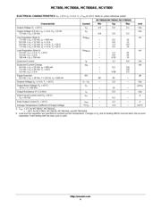
MAXIMUM RATINGS (T
A
= 25°C, unless otherwise noted)
Rating Symbo
l
Value
Unit
369C 221A
936
Input Voltage (5.0 − 18 V)
(24 V)
V
I
35
40
Vdc
Power Dissipation P
D
Internally Limited W
Thermal Resistance,
Junction−to−Ambient
R
q
JA
92 65 Figure
15
°C/W
Thermal Resistance,
Junction−to−Case
R
q
JC
5.0 5.0 5.0 °C/W
Storage Junction Temperature
Range
T
stg
−65 to +150 °C
Operating Junction Temperature T
J
+150 °C
Stresses exceeding those listed in the Maximum Ratings table may damage the
device. If any of these limits are exceeded, device functionality should not be
assumed, damage may occur and reliability may be affected.
*This device series contains ESD protection and exceeds the following tests:
Human Body Model 2000 V per MIL_STD_883, Method 3015.
Machine Model Method 200 V.
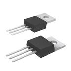
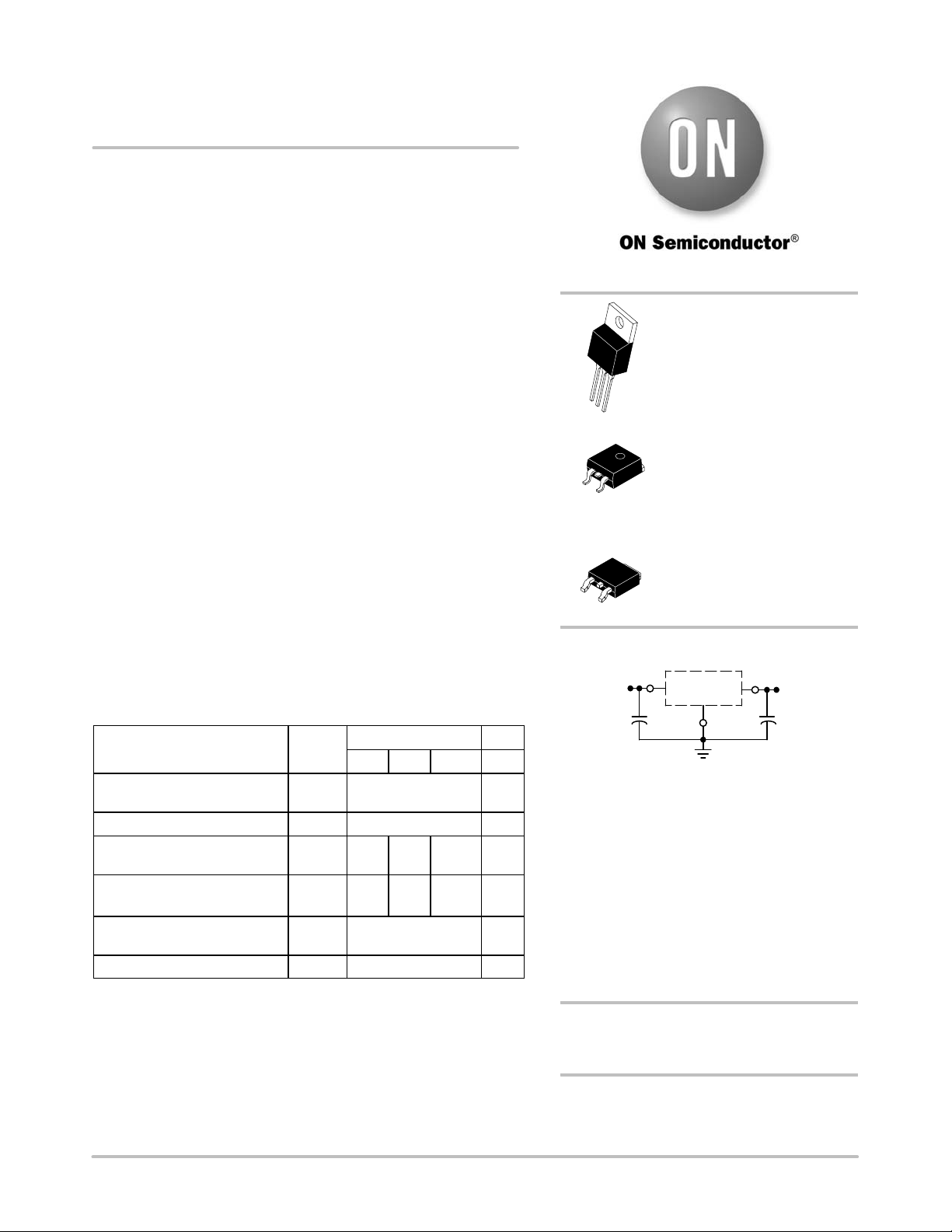
TO−220
T SUFFIX
CASE 221AB
1
D
2
PAK−3
D2T SUFFIX
CASE 936
2
3
See detailed ordering and shipping information in the packag
e
dimensions section on page 23 of this data sheet.
ORDERING INFORMATION
Heatsink surface
connected to Pin 2
.
Pin 1. Input
2. Ground
3. Output
Heatsink surface (shown as terminal 4 in
case outline drawing) is connected to Pin 2.
1
3
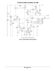
STANDARD APPLICATION
A common ground is required between the
input and the output voltages. The input voltage
must remain typically 2.0 V above the output
voltage even during the low point on the input
ripple voltage.
XX,
MC78XX
Input
C
in
*
0.33 mF
C
O
**
Output
These two digits of the type number
indicate nominal voltage.
C
in
is required if regulator is located an
appreciable distance from power supply
filter.
C
O
is not needed for stability; however,
it does improve transient response. Values
of less than 0.1 mF could cause instability.
*
**
See general marking information in the device markin
g
section on page 28 of this data sheet.
DEVICE MARKING INFORMATION
DPAK−3
DT SUFFIX
CASE 369C
http://onsemi.com
1
2
3
4
器件 Datasheet 文档搜索
AiEMA 数据库涵盖高达 72,405,303 个元件的数据手册,每天更新 5,000 多个 PDF 文件
