Datasheet 搜索 > 线性调节器 > National Semiconductor(美国国家半导体) > LM79L05ACMX 数据手册 > LM79L05ACMX 数据手册 3/8 页
 器件3D模型
¥ 1
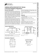
LM79L05ACMX 数据手册 - National Semiconductor(美国国家半导体)
制造商:
National Semiconductor(美国国家半导体)
分类:
线性调节器
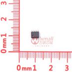
封装:
SOIC
描述:
LM79L05ACMX
Pictures:
3D模型
符号图
焊盘图
引脚图
产品图
页面导航:
导航目录
LM79L05ACMX数据手册
Page:
of 8 Go
若手册格式错乱,请下载阅览PDF原文件
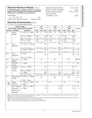
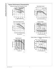
Absolute Maximum Ratings (Note 1)
If Military/Aerospace specified devices are required,
please contact the National Semiconductor Sales Office/
Distributors for availability and specifications.
Input Voltage
V
O
= −5V, −12V, −15V −35V
Internal Power Dissipation (Note 2) Internally Limited
Operating Temperature Range 0˚C to +70˚C
Maximum Junction Temperature +125˚C
Storage Temperature Range −55˚C to +150˚C
Lead Temperature
(Soldering, 10 sec.) 260˚C
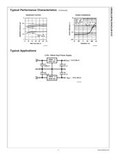
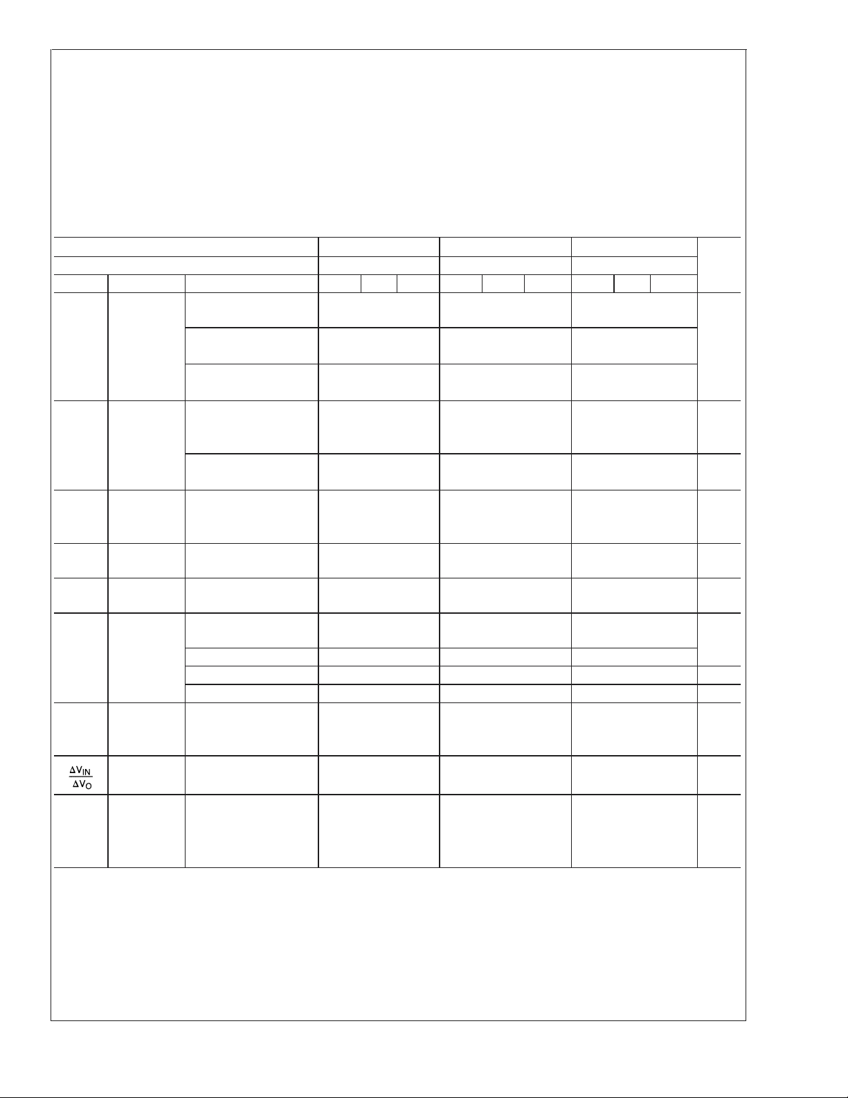
Electrical Characteristics (Note 3)
T
A
= 0˚C to +70˚C unless otherwise noted.
Output Voltage −5V −12V −15V
Input Voltage (unless otherwise noted) −10V −17V −20V Units
Symbol Parameter Conditions Min Typ Max Min Typ Max Min Typ Max
V
O
Output
Voltage
T
J
= 25˚C, I
O
= 100mA −5.2 −5 −4.8 −12.5 −12 −11.5 −15.6 −15 −14.4
1mA ≤ I
O
≤ 100mA −5.25 −4.75 −12.6 −11.4 −15.75 −14.25
V
MIN
≤ V
IN
≤ V
MAX
(−20 ≤ V
IN
≤ −7.5) (−27 ≤ V
IN
≤ −14.8) (−30 ≤ V
IN
≤ −18) V
1mA ≤ I
O
≤ 40mA −5.25 −4.75 −12.6 −11.4 −15.75 −14.25
V
MIN
≤ V
IN
≤ V
MAX
(−20 ≤ V
IN
≤ −7) (−27 ≤ V
IN
≤ −14.5) (−30 ≤ V
IN
≤ −17.5)
∆V
O
Line
Regulation
T
J
= 25˚C, I
O
= 100mA 60 45 45 mV
V
MIN
≤ V
IN
≤ V
MAX
(−20 ≤ V
IN
≤ −7.3) (−27 ≤ V
IN
≤ −14.6) (−30 ≤ V
IN
≤ −17.7) V
T
J
= 25˚C, I
O
= 40mA 60 45 45 mV
V
MIN
≤ V
IN
≤ V
MAX
(−20 ≤ V
IN
≤ −7) (−27 ≤ V
IN
≤ −14.5) (−30 ≤ V
IN
≤ −17.5) V
∆V
O
Load
Regulation
T
J
= 25˚C
50 100 125 mV
1mA ≤ I
O
≤ 100mA
∆V
O
Long Term
Stability
I
O
= 100mA 20 48 60 mV/khrs
I
Q
Quiescent
Current
I
O
= 100mA 2 6 2 6 2 6 mA
∆I
Q
Quiescent
Current
1mA ≤ I
O
≤ 100mA 0.3 0.3 0.3
Change 1mA ≤ I
O
≤ 40mA 0.1 0.1 0.1 mA
I
O
= 100mA 0.25 0.25 0.25 mA
V
MIN
≤ V
IN
≤ V
MAX
(−20 ≤ V
IN
≤ −7.5) (−27 ≤ V
IN
≤ −14.8) (−30 ≤ V
IN
≤ −18) V
V
n
Output Noise
Voltage
T
J
= 25˚C, I
O
= 100mA
40 96 120 µV
f = 10Hz − 10kHz
Ripple
Rejection
T
J
= 25˚C, I
O
= 100mA
50 52 50 dB
f = 120Hz
Input Voltage T
J
= 25˚C, I
O
= 100mA −7.3 −14.6 −17.7 V
Required to I
O
= 40mA −7.0 −14.5 −17.5 V
Maintain Line
Regulation
Note 1: Absolute Maximum Ratings indicate limits beyond which damage to the device may occur. Operating Ratings indicate conditions for which the device is
functional, but do not guarantee specific performance limits.
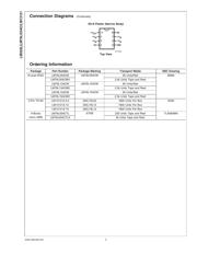
Note 2: Thermal resistance of Z package is 60˚C/W θ
JC
, 232˚C/W θ
JA
at still air, and 88˚C/W at 400 ft/min of air. The M package θ
JA
is 180˚C/W in still air. The
maximum junction temperature shall not exceed 125˚C on electrical parameters.
Note 3: To ensure constant junction temperature, low duty cycle pulse testing is used.
LM320L/LM79LXXAC/LM13121
www.national.com3
器件 Datasheet 文档搜索
AiEMA 数据库涵盖高达 72,405,303 个元件的数据手册,每天更新 5,000 多个 PDF 文件
