Datasheet 搜索 > 时钟信号器件 > TI(德州仪器) > LMC555CM/NOPB 数据手册 > LMC555CM/NOPB 数据手册 1/25 页
 器件3D模型
¥ 4.813
LMC555CM/NOPB 数据手册 - TI(德州仪器)
制造商:
TI(德州仪器)
分类:
时钟信号器件
封装:
SOIC-8
描述:
TEXAS INSTRUMENTS LMC555CM/NOPB 芯片, 定时器, 15V, SMD
Pictures:
3D模型
符号图
焊盘图
引脚图
产品图
页面导航:
封装尺寸在P11P12P14P15
标记信息在P11P12P13
封装信息在P2P11P12P13P14P15
应用领域在P1P13P25
导航目录
LMC555CM/NOPB数据手册
Page:
of 25 Go
若手册格式错乱,请下载阅览PDF原文件
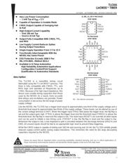
SLFS043F − SEPTEMBER 1983 − REVISED FEBRUARY 2005
1
POST OFFICE BOX 655303 • DALLAS, TEXAS 75265
D Very Low Power Consumption
− 1 mW Typ at V
DD
= 5 V
D Capable of Operation in Astable Mode
D CMOS Output Capable of Swinging Rail
to Rail
D High Output-Current Capability
− Sink 100 mA Typ
− Source 10 mA Typ
D Output Fully Compatible With CMOS, TTL,
and MOS
D Low Supply Current Reduces Spikes
During Output Transitions
D Single-Supply Operation From 2 V to 15 V
D Functionally Interchangeable With the
NE555; Has Same Pinout
D ESD Protection Exceeds 2000 V Per
MIL-STD-883C, Method 3015.2
D Available in Q-Temp Automotive
High Reliability Automotive Applications
Configuration Control/Print Support
Qualification to Automotive Standards
description
The TLC555 is a monolithic timing circuit
fabricated using the TI LinCMOS process. The
timer is fully compatible with CMOS, TTL, and
MOS logic and operates at frequencies up to
2 MHz. Because of its high input impedance, this
device uses smaller timing capacitors than those
used by the NE555. As a result, more accurate
time delays and oscillations are possible. Power
consumption is low across the full range of power
supply voltage.
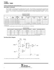
Like the NE555, the TLC555 has a trigger level equal to approximately one-third of the supply voltage and a
threshold level equal to approximately two-thirds of the supply voltage. These levels can be altered by use of
the control voltage terminal (CONT). When the trigger input (TRIG) falls below the trigger level, the flip-flop is
set and the output goes high. If TRIG is above the trigger level and the threshold input (THRES) is above the
threshold level, the flip-flop is reset and the output is low. The reset input (RESET) can override all other inputs
and can be used to initiate a new timing cycle. If RESET is low, the flip-flop is reset and the output is low.
Whenever the output is low, a low-impedance path is provided between the discharge terminal (DISCH) and
GND. All unused inputs should be tied to an appropriate logic level to prevent false triggering.
While the CMOS output is capable of sinking over 100 mA and sourcing over 10 mA, the TLC555 exhibits greatly
reduced supply-current spikes during output transitions. This minimizes the need for the large decoupling
capacitors required by the NE555.
Please be aware that an important notice concerning availability, standard warranty, and use in critical applications of
Texas Instruments semiconductor products and disclaimers thereto appears at the end of this data sheet.
Copyright 1983−2005, Texas Instruments Incorporated
!
" #
$%! & %
& !
LinCMOS is a trademark of Texas Instruments.
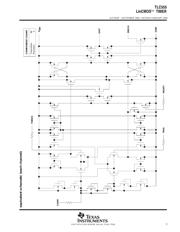
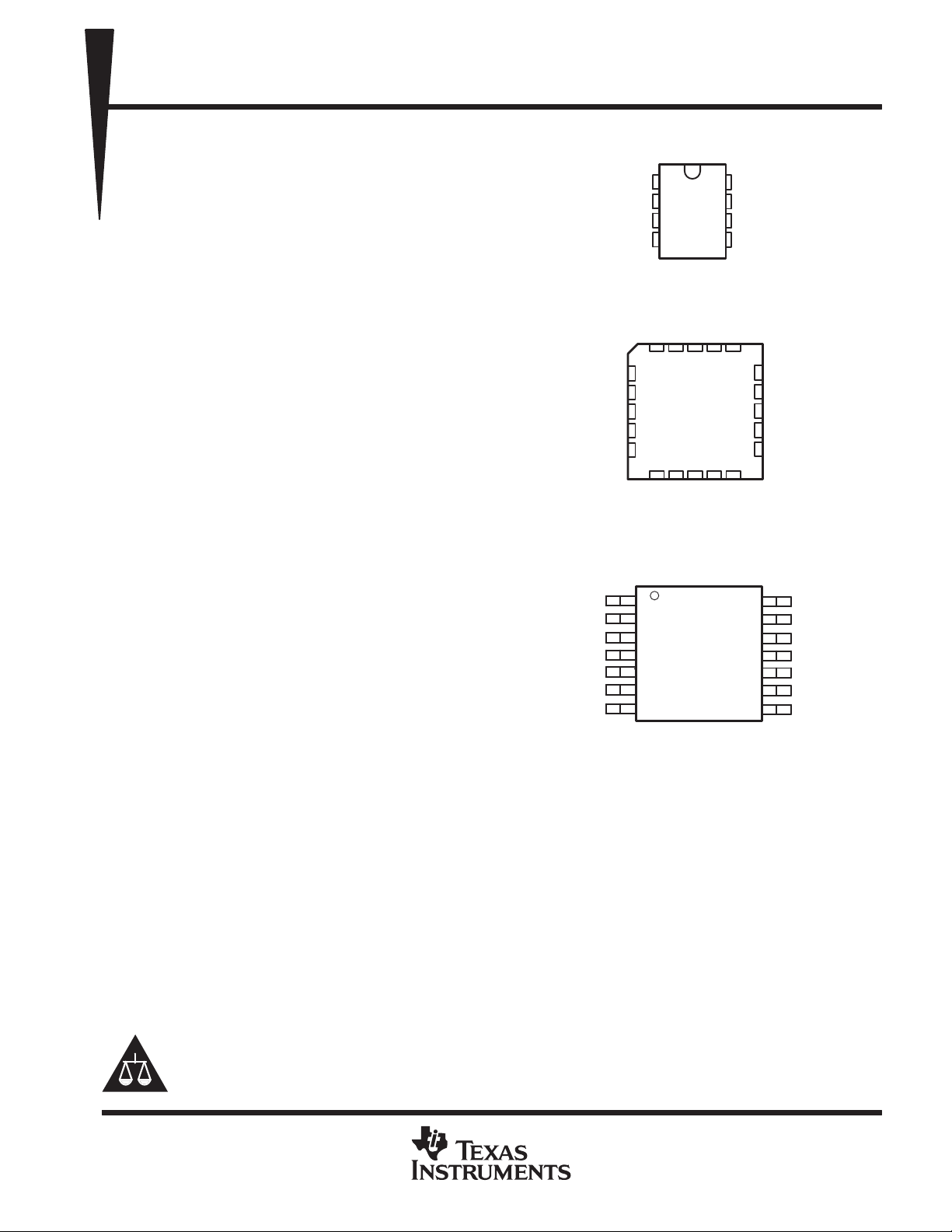
3212019
910111213
4
5
6
7
8
18
17
16
15
14
NC
DISCH
NC
THRES
NC
NC
TRIG
NC
OUT
NC
FK PACKAGE
(TOP VIEW)
NC
GND
NC
CONT
NC
V
NC
RESET
NC
NC
DD
D, DB, JG, OR P PACKAGE
(TOP VIEW)
1
2
3
4
8
7
6
5
GND
TRIG
OUT
RESET
V
DD
DISCH
THRES
CONT
NC − No internal connection
1
2
3
4
5
6
7
14
13
12
11
10
9
8
GND
NC
TRIG
NC
OUT
NC
RESET
V
DD
NC
DISCH
NC
THRES
NC
CONT
PW PACKAGE
(TOP VIEW)
'(')*)+
"$ ! " +
& % & !
器件 Datasheet 文档搜索
AiEMA 数据库涵盖高达 72,405,303 个元件的数据手册,每天更新 5,000 多个 PDF 文件
