Datasheet 搜索 > National Semiconductor(美国国家半导体) > LMC7111BIM5/NOPB 数据手册 > LMC7111BIM5/NOPB 数据手册 6/21 页

¥ 3.363
LMC7111BIM5/NOPB 数据手册 - National Semiconductor(美国国家半导体)
制造商:
National Semiconductor(美国国家半导体)
封装:
SOT-23-5
Pictures:
3D模型
符号图
焊盘图
引脚图
产品图
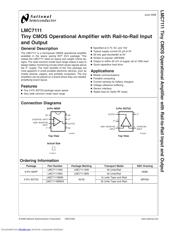
LMC7111BIM5/NOPB数据手册
Page:
of 21 Go
若手册格式错乱,请下载阅览PDF原文件
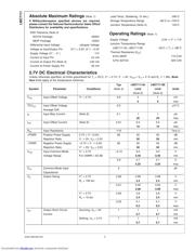
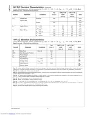
10V DC Electrical Characteristics (Continued)
Unless otherwise specified, all limits guaranteed for T
J
= 25˚C, V
+
= 10V, V
−
= 0V, V
CM
=V
O
=V
+
/2 and R
L
>
1MΩ. Bold-
face limits apply at the temperature extremes.
Typ LMC7111AI LMC7111BI
Symbol Parameter Conditions (Note 5) Limit Limit Units
(Note 6) (Note 6)
A
VOL
Voltage Gain Sourcing 500 V/mv
100 kΩ Load min
Sinking 200 V/mv
min
I
S
Supply Current V
+
= +10V, 25 50 60 µA
V
O
=V
+
/2 65 75 max
V
O
Output Swing V
+
= 10V 9.99 9.98 9.98 Vmin
R
L
= 100 kΩ 0.01 0.02 0.02 Vmax
V
+
= 10V 9.98 9.9 9.9 Vmin
R
L
=10kΩ 0.02 0.1 0.1 Vmin
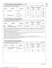
10V AC Electrical Characteristics
Unless otherwise specified, all limits guaranteed for T
J
= 25˚C, V
+
= 10V, V
−
= 0V, V
CM
=V
O
=V
+
/2 and R
L
>
1MΩ. Bold-
face limits apply at the temperature extremes.
Typ LMC7111AI LMC7111BI
Symbol Parameter Conditions (Note 5) Limit Limit Units
(Note 6) (Note 6)
SR Slew Rate (Note 8) 0.03 V/µs
GBW Gain-Bandwidth Product 50 kHz
φ
m
Phase Margin 50 deg
G
m
Gain Margin 15 dB
Input-Referred f = 1 kHz 110
Voltage Noise V
CM
=1V
Input-Referred f = 1 kHz 0.03
Current Noise
Note 19: Absolute Maximum Ratings indicate limits beyond which damage to the device may occur. Operating Ratings indicate conditions for which the device is
intended to be functional, but specific performance is not guaranteed. For guaranteed specifications and the test conditions, see the Electrical Characteristics.
Note 20: Human body model, 1.5 kΩ in series with 100 pF.
Note 21: Applies to both single-supply and split-supply operation. Continuous short circuit operation at elevated ambient temperature can result in exceeding the
maximum allowed junction temperature at 150˚C.
Note 22: The maximum power dissipation is a function of T
J(max)
, θ
JA
and T
A
. The maximum allowable power dissipation at any ambient temperature is P
D
=
(T
J(max)
−T
A
)/θ
JA
. All numbers apply for packages soldered directly into a PC board.
Note 23: Typical Values represent the most likely parametric norm.
Note 24: All limits are guaranteed by testing or statistical analysis.
Note 25: V
+
= 10V, V
CM
= 5V and R
L
connected to 5V. For Sourcing tests, 5V ≤ V
O
≤ 10V. For Sinking tests, 0.5V ≤ V
O
≤ 5V.
Note 26: Connected as Voltage Follower with 1.0V step input. Number specified is the slower of the positive and negative slew rates. Input referred, V
+
= 10V and
R
L
= 100 kΩ connected to 5V. Amp excited with 1 kHz to produce V
O
=2V
PP
.
Note 27: Operation near absolute maximum limits will adversely affect reliability.
LMC7111
www.national.com 6
Downloaded from Elcodis.com electronic components distributor
器件 Datasheet 文档搜索
AiEMA 数据库涵盖高达 72,405,303 个元件的数据手册,每天更新 5,000 多个 PDF 文件
