Datasheet 搜索 > 稳压芯片 > TI(德州仪器) > LP3966ES-ADJ/NOPB 数据手册 > LP3966ES-ADJ/NOPB 数据手册 4/25 页

¥ 24.652
LP3966ES-ADJ/NOPB 数据手册 - TI(德州仪器)
制造商:
TI(德州仪器)
分类:
稳压芯片
封装:
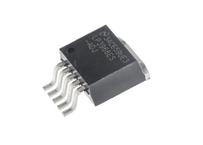
TO-263-6
描述:
TEXAS INSTRUMENTS LP3966ES-ADJ/NOPB 电压稳压器, LDO, 可调, 2.5V至7V输入, 80mV压差, 1.215V至5.1V/3A输出, TO-263-5
Pictures:
3D模型
符号图
焊盘图
引脚图
产品图
页面导航:
引脚图在P4Hot
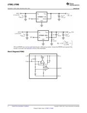
典型应用电路图在P1
原理图在P2P3
封装尺寸在P18P19P21P22
标记信息在P18P19
封装信息在P18P19P20P21P22
技术参数、封装参数在P4
应用领域在P1P25
电气规格在P4P5P6P7P8P9P13P14

导航目录
LP3966ES-ADJ/NOPB数据手册
Page:
of 25 Go
若手册格式错乱,请下载阅览PDF原文件
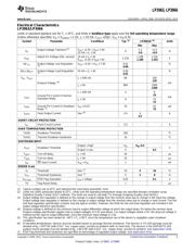
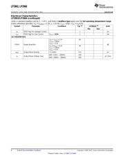
LP3963, LP3966
SNVS067H –APRIL 2000–REVISED APRIL 2013
www.ti.com
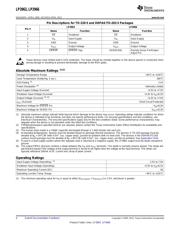
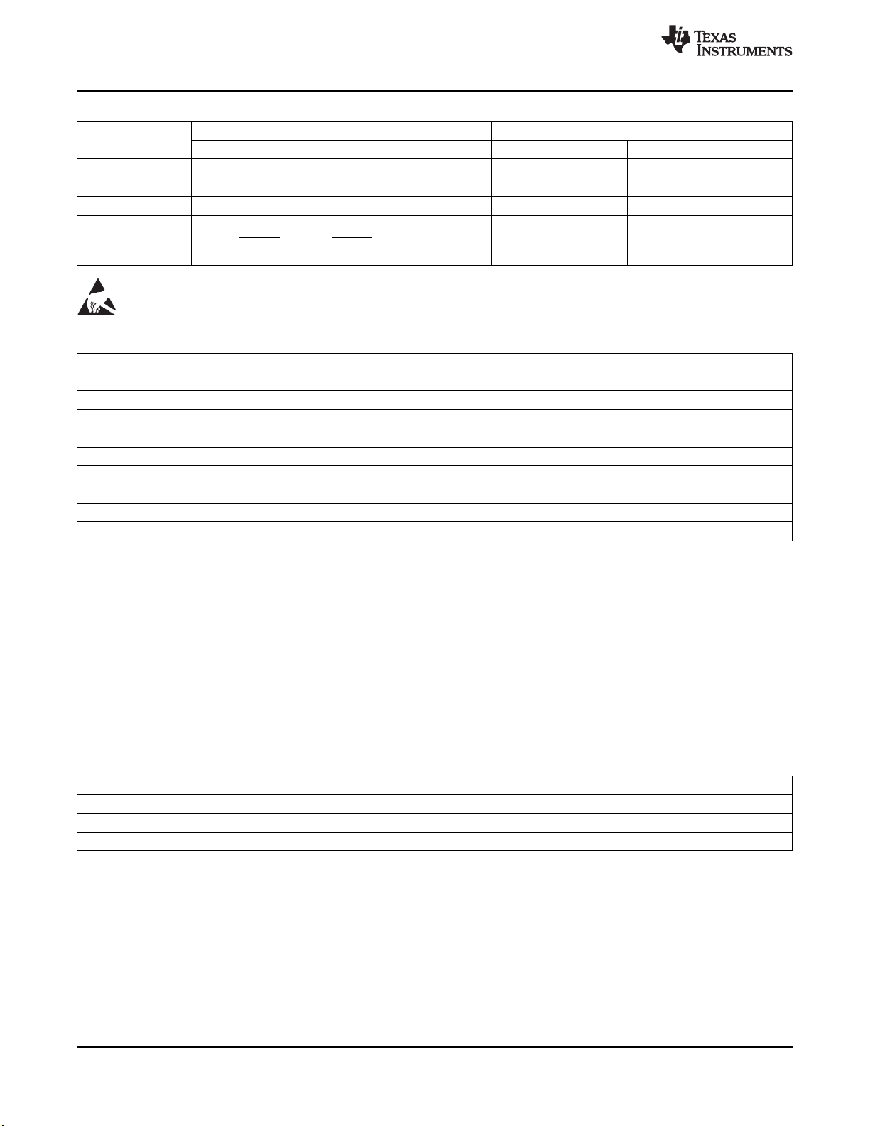
Pin Descriptions for TO-220-5 and DDPAK/TO-263-5 Packages
LP3963 LP3966
Pin #
Name Function Name Function
1 SD Shutdown SD Shutdown
2 V
IN
Input Supply V
IN
Input Supply
3 GND Ground GND Ground
4 V
OUT
Output Voltage V
OUT
Output Voltage
5 ERROR ERROR Flag SENSE/ADJ Remote Sense Pin/Output
Adjust Pin
These devices have limited built-in ESD protection. The leads should be shorted together or the device placed in conductive foam
during storage or handling to prevent electrostatic damage to the MOS gates.
Absolute Maximum Ratings
(1)(2)
Storage Temperature Range −65°C to +150°C
Lead Temperature (Soldering, 5 sec.) 260°C
ESD Rating
(3)
2 kV
Power Dissipation
(4)
Internally Limited
Input Supply Voltage (Survival) −0.3V to +7.5V
Shutdown Input Voltage (Survival) −0.3V to V
IN
+0.3V
Output Voltage (Survival)
(5) (6)
−0.3V to +7.5V
I
OUT
(Survival) Short Circuit Protected
Maximum Voltage for ERROR Pin V
IN
+0.3V
Maximum Voltage for SENSE Pin V
OUT
+0.3V
(1) Absolute maximum ratings indicate limits beyond which damage to the device may occur. Operating ratings indicate conditions for which
the device is intended to be functional, but does not specify performance limits. For ensured specifications and test conditions, see
Electrical Characteristics. The ensured specifications apply only for the test conditions listed. Some performance characteristics may
degrade when the device is not operated under the listed test conditions.
(2) If Military/Aerospace specified devices are required, please contact the Texas Instruments Sales Office/ Distributors for availability and
specifications.
(3) The human body model is a 100pF capacitor discharged through a 1.5kΩ resistor into each pin.
(4) At elevated temperatures, devices must be derated based on package thermal resistance. The devices in TO-220 package must be
derated at θ
jA
= 50°C/W (with 0.5in
2
, 1oz. copper area), junction-to-ambient (with no heat sink). The devices in the DDPAK/TO-263
surface-mount package must be derated at θ
jA
= 60°C/W (with 0.5in
2
, 1oz. copper area), junction-to-ambient. See Application Hints.
(5) If used in a dual-supply system where the regulator load is returned to a negative supply, the LP396X output must be diode-clamped to
ground.
(6) The output PMOS structure contains a diode between the V
IN
and V
OUT
terminals. This diode is normally reverse biased. This diode will
get forward biased if the voltage at the output terminal is forced to be higher than the voltage at the input terminal. This diode can
typically withstand 200mA of DC current and 1Amp of peak current.
Operating Ratings
Input Supply Voltage (Operating),
(1)
2.5V to 7.0V
Shutdown Input Voltage (Operating) −0.3V to V
IN
+0.3V
Maximum Operating Current (DC) 3A
Operating Junction Temp. Range −40°C to +125°C
(1) The minimum operating value for V
IN
is equal to either [V
OUT(NOM)
+ V
DROPOUT
] or 2.5V, whichever is greater.
4 Submit Documentation Feedback Copyright © 2000–2013, Texas Instruments Incorporated
Product Folder Links: LP3963 LP3966
器件 Datasheet 文档搜索
AiEMA 数据库涵盖高达 72,405,303 个元件的数据手册,每天更新 5,000 多个 PDF 文件
