Datasheet 搜索 > 稳压芯片 > TI(德州仪器) > LP5907UVX-1.8/NOPB 数据手册 > LP5907UVX-1.8/NOPB 数据手册 6/36 页

¥ 0.835
LP5907UVX-1.8/NOPB 数据手册 - TI(德州仪器)
制造商:
TI(德州仪器)
分类:
稳压芯片
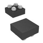
封装:
XFBGA-4
描述:
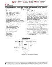
超低噪音, 250毫安线性稳压器的射频/模拟电路 - 无需旁路电容 Ultra Low-Noise, 250 mA Linear Regulator for RF/Analog Circuits - Requires No Bypass Capacitor
Pictures:
3D模型
符号图
焊盘图
引脚图
产品图
页面导航:
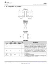
引脚图在P3Hot
典型应用电路图在P13
原理图在P1P11
封装尺寸在P20P23P24P25P27P28P29P30P33
焊盘布局在P21P34
标记信息在P23P24P25P26
封装信息在P19P23P24P25P26P27P28P29P30
技术参数、封装参数在P4
应用领域在P1P4P5P13P36
电气规格在P5P6P15
导航目录
LP5907UVX-1.8/NOPB数据手册
Page:
of 36 Go
若手册格式错乱,请下载阅览PDF原文件
6
LP5907
SNVS798J –APRIL 2012–REVISED MARCH 2016
www.ti.com
Product Folder Links: LP5907
Submit Documentation Feedback Copyright © 2012–2016, Texas Instruments Incorporated
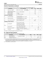
Electrical Characteristics (continued)
V
IN
= V
OUT(NOM)
+ 1 V, V
EN
= 1.2 V, I
OUT
= 1 mA, C
IN
= 1 µF, C
OUT
= 1 µF, unless otherwise stated.
(1)(2)(3)
PARAMETER TEST CONDITIONS MIN TYP MAX UNIT
(10) There is a 1-MΩ resistor between EN and ground on the device.
e
N
Output noise voltage
(9)
BW = 10 Hz to 100 kHz
I
OUT
= 1 mA 10
µV
RMS
I
OUT
= 250 mA 6.5
R
AD
Output Automatic Discharge
pulldown resistance
V
EN
< V
IL
(output disabled) 230 Ω
T
SD
Thermal shutdown T
J
rising 160
°C
Thermal hysteresis T
J
falling from shutdown 15
LOGIC INPUT THRESHOLDS
V
IL
Low input threshold
V
IN
= 2.2 V to 5.5 V
V
EN
falling until the output is disabled
0.4 V
V
IH
High input threshold
V
IN
= 2.2 V to 5.5 V
V
EN
rising until the output is enabled
1.2 V
I
EN
Input current at EN pin
(10)
V
EN
= 5.5 V and V
IN
= 5.5 V 5.5
µA
V
EN
= 0 V and V
IN
= 5.5 V 0.001
TRANSIENT CHARACTERISTICS
ΔV
OUT
Line transient
(9)
V
IN
= (V
OUT(NOM)
+ 1 V) to
(V
OUT(NOM
) + 1.6 V) in 30 µs
–1
mV
V
IN
= (V
OUT(NOM)
+ 1.6 V) to
(V
OUT(NOM
) + 1.6 V) in 30 µs
1
Load transient
(9)
I
OUT
= 1 mA to 250 mA in 10 µs –40
mV
I
OUT
= 250 mA to 1mA in 10 µs 40
Overshoot on start-up
(9)
Stated as a percentage of V
OUT(NOM)
5%
t
ON
Turnon time
From V
EN
> V
IH
to V
OUT
= 95% of V
OUT(NOM)
T
A
= 25°C
80 150 µs
(1) The minimum capacitance should be greater than 0.5 μF over the full range of operating conditions. The capacitor tolerance should be
30% or better over the full temperature range. The full range of operating conditions for the capacitor in the application must be
considered during device selection to ensure this minimum capacitance specification is met. X7R capacitors are recommended however
capacitor types X5R, Y5V and Z5U may be used with consideration of the application and conditions.
(2) This specification is verified by design.
6.6 Output and Input Capacitors
over operating free-air temperature range (unless otherwise noted)
PARAMETER TEST CONDITIONS MIN
(1)
TYP MAX UNIT
C
IN
Input capacitance
(2)
Capacitance for stability
0.7 1 µF
C
OUT
Output capacitance
(2)
0.7 1 10 µF
ESR Output/Input capacitance
(2)
5 500 mΩ
器件 Datasheet 文档搜索
AiEMA 数据库涵盖高达 72,405,303 个元件的数据手册,每天更新 5,000 多个 PDF 文件
