Datasheet 搜索 > 微控制器 > NXP(恩智浦) > LPC1343FBD48,151 数据手册 > LPC1343FBD48,151 数据手册 2/74 页
 器件3D模型
¥ 36.977
LPC1343FBD48,151 数据手册 - NXP(恩智浦)
制造商:
NXP(恩智浦)
分类:
微控制器
封装:
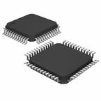
LQFP-48
描述:
ARM Cortex-M3 Microcontrollers, NXP基于 NXP ARM Cortex-M3 的微控制器,适用于嵌入式应用,具有高集成水平并提供系统增强功能,例如低功耗、增强调试功能和更高级别的块集成支持。Cortex-M3 核可最高以 150 MHz 运行 高达 512KB 的闪存和高达 64KB 的片上 SRAM 低功耗,用于 LPC13xx 设备时低至 200μA/MHz 新唤醒中断控制器 (WIC)、套放向量中断控制器 (NVIC) 和存储器保护装置 配有先进的外围设备,如以太网、USB 主机/OTG/设备、CAN、IS、快速模式 Plus (Fm+) IC、12 位 ADC、电机控制 PWM、正交编码器接口和其他。 ### ARM Cortex 微控制器,NXP
Pictures:
3D模型
符号图
焊盘图
引脚图
产品图
页面导航:
导航目录
LPC1343FBD48,151数据手册
Page:
of 74 Go
若手册格式错乱,请下载阅览PDF原文件

LPC1311_13_42_43 All information provided in this document is subject to legal disclaimers. © NXP B.V. 2012. All rights reserved.
Product data sheet Rev. 5 — 6 June 2012 2 of 74
NXP Semiconductors
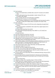
LPC1311/13/42/43
32-bit ARM Cortex-M3 microcontroller
Serial interfaces:
USB 2.0 full-speed device controller with on-chip PHY for device (LPC1342/43
only).
UART with fractional baud rate generation, modem, internal FIFO, and
RS-485/EIA-485 support.
SSP controller with FIFO and multi-protocol capabilities.
Additional SSP controller on LPC1313FBD48/01.
I
2
C-bus interface supporting full I
2
C-bus specification and Fast-mode Plus with a
data rate of 1 Mbit/s with multiple address recognition and monitor mode.
Other peripherals:
Up to 42 General Purpose I/O (GPIO) pins with configurable pull-up/pull-down
resistors.
Four general purpose counter/timers with a total of four capture inputs and 13
match outputs.
Programmable WatchDog Timer (WDT).
Programmable Windowed Watchdog Timer (WWDT) on LPC1311/01 and
LPC1313/01.
System tick timer.
Serial Wire Debug and Serial Wire Trace port.
High-current output driver (20 mA) on one pin.
High-current sink drivers (20 mA) on two I
2
C-bus pins in Fast-mode Plus.
Integrated PMU (Power Management Unit) to minimize power consumption during
Sleep, Deep-sleep, and Deep power-down modes.
Power profiles residing in boot ROM allowing to optimize performance and minimize
power consumption for any given application through one simple function call.
(LPC1300L series, on LPC1311/01 and LPC1313/01 only.)
Three reduced power modes: Sleep, Deep-sleep, and Deep power-down.
Single power supply (2.0 V to 3.6 V).
10-bit ADC with input multiplexing among 8 pins.
GPIO pins can be used as edge and level sensitive interrupt sources.
Clock output function with divider that can reflect the system oscillator clock, IRC
clock, CPU clock, or the watchdog clock.
Processor wake-up from Deep-sleep mode via a dedicated start logic using up to 40 of
the functional pins.
Brownout detect with four separate thresholds for interrupt and one threshold for
forced reset (four thresholds for forced reset on the LPC1311/01 and LPC1313/01
parts).
Power-On Reset (POR).
Integrated oscillator with an operating range of 1 MHz to 25 MHz.
12 MHz internal RC oscillator trimmed to 1 % accuracy over the entire temperature
and voltage range that can optionally be used as a system clock.
Programmable watchdog oscillator with a frequency range of 7.8 kHz to 1.8 MHz.
System PLL allows CPU operation up to the maximum CPU rate without the need for a
high-frequency crystal. May be run from the system oscillator or the internal RC
oscillator.
For USB (LPC1342/43), a second, dedicated PLL is provided.
Code Read Protection (CRP) with different security levels.
器件 Datasheet 文档搜索
AiEMA 数据库涵盖高达 72,405,303 个元件的数据手册,每天更新 5,000 多个 PDF 文件
