Datasheet 搜索 > 电压基准芯片 > TI(德州仪器) > LT1004CDRG4-2-5 数据手册 > LT1004CDRG4-2-5 数据手册 4/63 页
 器件3D模型
¥ 2.353
LT1004CDRG4-2-5 数据手册 - TI(德州仪器)
制造商:
TI(德州仪器)
分类:
电压基准芯片
封装:
SOIC-8
描述:
2.5V 微功耗集成精密基准电压 8-SOIC 0 to 70
Pictures:
3D模型
符号图
焊盘图
引脚图
产品图
页面导航:
封装尺寸在P2P49P50P51P52P53P54
型号编码规则在P2
标记信息在P2P49P50P51P52
封装信息在P49P50P51P52P53P54
导航目录
LT1004CDRG4-2-5数据手册
Page:
of 63 Go
若手册格式错乱,请下载阅览PDF原文件
TL05x, TL05xA
ENHANCED-JFET LOW-OFFSET
OPERATIONAL AMPLIFIERS
SLOS178A – FEBRUARY 1997 - REVISED FEBRUARY 2003
4
POST OFFICE BOX 655303 • DALLAS, TEXAS 75265
absolute maximum ratings over operating free-air temperature range (unless otherwise noted)
†
Supply voltage, V
CC+
(see Note 1) 18 V. . . . . . . . . . . . . . . . . . . . . . . . . . . . . . . . . . . . . . . . . . . . . . . . . . . . . . . . . . .
Supply voltage, V
CC–
(see Note 1) –18 V. . . . . . . . . . . . . . . . . . . . . . . . . . . . . . . . . . . . . . . . . . . . . . . . . . . . . . . . . .
Differential input voltage (see Note 2) ±30 V. . . . . . . . . . . . . . . . . . . . . . . . . . . . . . . . . . . . . . . . . . . . . . . . . . . . . . . .
Input voltage range, V
I
(any input, see Notes 1 and 3) ±15 V. . . . . . . . . . . . . . . . . . . . . . . . . . . . . . . . . . . . . . . . .
Input current, I
I
(each input) ±1 mA. . . . . . . . . . . . . . . . . . . . . . . . . . . . . . . . . . . . . . . . . . . . . . . . . . . . . . . . . . . . . . .
Output current, I
O
(each output) ±80 mA. . . . . . . . . . . . . . . . . . . . . . . . . . . . . . . . . . . . . . . . . . . . . . . . . . . . . . . . . .
Total current into V
CC+
160 mA. . . . . . . . . . . . . . . . . . . . . . . . . . . . . . . . . . . . . . . . . . . . . . . . . . . . . . . . . . . . . . . . . .
Total current out of V
CC–
160 mA. . . . . . . . . . . . . . . . . . . . . . . . . . . . . . . . . . . . . . . . . . . . . . . . . . . . . . . . . . . . . . . . .
Duration of short-circuit current at (or below) 25°C Unlimited. . . . . . . . . . . . . . . . . . . . . . . . . . . . . . . . . . . . . . . . .
Package thermal impedance, θ
JA
(see Notes 4 and 5): D package (8 pin) 97°C/W. . . . . . . . . . . . . . . . . . . . . .
D package (14 pin) 86°C/W. . . . . . . . . . . . . . . . . . . . .
DB package (14 pin) 96°C/W. . . . . . . . . . . . . . . . . . .
N package (14 pin) 80°C/W. . . . . . . . . . . . . . . . . . . . .
NS package (14 pin) 76°C/W. . . . . . . . . . . . . . . . . . .
P package (8 pin) 85°C/W. . . . . . . . . . . . . . . . . . . . . .
PS package (8 pin) 95°C/W. . . . . . . . . . . . . . . . . . . .
Operating virtual junction temperature, T
J
150°C. . . . . . . . . . . . . . . . . . . . . . . . . . . . . . . . . . . . . . . . . . . . . . . . . . .
Lead temperature 1,6 mm (1/16inch) from case for 10 seconds 260°C. . . . . . . . . . . . . . . . . . . . . . . . . . . . . . . .
Storage temperature range –65°C to 150°C. . . . . . . . . . . . . . . . . . . . . . . . . . . . . . . . . . . . . . . . . . . . . . . . . . . . . . . .
†
Stresses beyond those listed under “absolute maximum ratings” may cause permanent damage to the device. These are stress ratings only, and
functional operation of the device at these or any other conditions beyond those indicated under “recommended operating conditions” is not
implied. Exposure to absolute-maximum-rated conditions for extended periods may affect device reliability.
NOTES: 1. All voltage values, except differential voltages, are with respect to the midpoint between V
CC+
and V
CC–.
2. Differential voltages are at IN+ with respect to IN–.
3. The magnitude of the input voltage must never exceed the magnitude of the supply voltage or 15 V, whichever is less.
4. Maximum power dissipation is a function of T
J
(max),
θ
JA
, and T
A
. The maximum allowable power dissipation at any allowable
ambient temperature is P
D
= (T
J
(max) – T
A
)/
θ
JA
. Operating at the absolute maximum T
J
of 150°C can impact reliability.
5. The package thermal impedance is calculated in accordance with JESD 51-7.
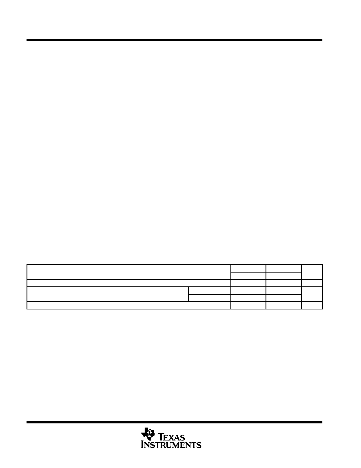
recommended operating conditions
C SUFFIX I SUFFIX
UNIT
MIN MAX MIN MAX
UNIT
V
CC±
Supply voltage ±5 ±15 ±5 ±15 V
V
IC
Common mode in
p
ut voltage
V
CC±
= ±5 V –1 4 –1 4
V
V
IC
Common
-
mode
input
voltage
V
CC±
= ±15 V –11 11 –11 11
V
T
A
Operating free-air temperature 0 70 –40 85 °C
器件 Datasheet 文档搜索
AiEMA 数据库涵盖高达 72,405,303 个元件的数据手册,每天更新 5,000 多个 PDF 文件
