Datasheet 搜索 > ADI(亚德诺) > LT1008S8#PBF 数据手册 > LT1008S8#PBF 数据手册 4/16 页
 器件3D模型
¥ 56.313
LT1008S8#PBF 数据手册 - ADI(亚德诺)
制造商:
ADI(亚德诺)
封装:
SOP
描述:
通用-放大器-1-电路-8-SO
Pictures:
3D模型
符号图
焊盘图
引脚图
产品图
页面导航:
封装尺寸在P14
焊盘布局在P15
技术参数、封装参数在P4
电气规格在P3P4
导航目录
LT1008S8#PBF数据手册
Page:
of 16 Go
若手册格式错乱,请下载阅览PDF原文件
4
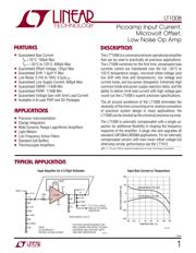
LT1008
1008fb
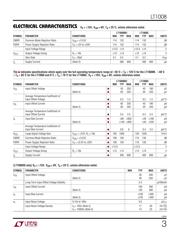
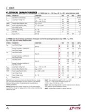
SYMBOL PARAMETER CONDITIONS MIN TYP MAX UNITS
i
n
Input Noise Current Density f
O
= 10Hz 20 fA/√Hz
A
VOL
Large-Signal Voltage Gain V
OUT
= ±12V, R
L
≥ 10k 200 2000 V/mV
V
OUT
= ±10V, R
L
≥ 2k 120 600 V/mV
CMRR Common Mode Rejection Ratio V
CM
= ±13.5V 110 132 dB
PSRR Power Supply Rejection Ratio V
S
= ±2V to ±20V 110 132 dB
Input Voltage Range ±13.5 ±14 V
V
OUT
Output Voltage Swing R
L
= 10k ±13 ±14 V
Slew Rate C
F
= 30pF 0.1 0.2 V/μs
I
S
Supply Current (Note 3) 380 600 μA
ELECTRICAL CHARACTERISTICS
(LT1008S8 only) V
S
= ±15V, V
CM
= 0V, T
A
= 25°C, unless otherwise noted.
(LT1008S8 only) The ● indicates specifications which apply over the full operating temperature range of 0°C ≤ T
A
≤ 70°C.
V
S
= ±15V, V
CM
= 0V, unless otherwise noted.
SYMBOL PARAMETER CONDITIONS MIN TYP MAX UNITS
V
OS
Input Offset Voltage ● 40 280 μV
(Note 3)
● 50 340 μV
Average Temperature Coefficient of ● 0.2 1.8 μV/°C
Input Offset Voltage
I
OS
Input Offset Current ● 120 380 pA
(Note 3)
● 140 500 pA
Average Temperature Coefficient of ● 0.4 4 pA/°C
Input Offset Current
I
B
Input Bias Current ● ±120 ±420 pA
(Note 3)
● ±140 ±550 pA
Average Temperature Coefficient of ● 0.4 5 pA/°C
Input Bias Current
A
VOL
Large-Signal Voltage Gain V
OUT
= ±12V, R
L
≥ 10k ● 150 1500 V/mV
CMRR Common Mode Rejection Ratio V
CM
= ±13.5V ● 108 130 dB
PSRR Power Supply Rejection Ratio V
S
= ±2.5V to ±20V ● 108 128 dB
Input Voltage Range ● ±13.5 V
V
OUT
Output Voltage Swing R
L
= 10k ● ±13 ±14 V
I
S
Supply Current ● 400 800 μA
Note 1:Stresses beyond those listed under Absolute Maximum Ratings
may cause permanent damage to the device. Exposure to any Absolute
Maximum Rating condition for extended periods may affect device
reliability and lifetime.
Note 2: Differential input voltages greater than 1V will cause excessive
current to flow through the input protection diodes unless current limiting
resistors are used.
Note 3: These specifications apply for ±2V ≤ V
S
≤ ±20V
(±2.5V ≤ V
S
≤ ±20V over the temperature range) and
–13.5V ≤ V
CM
≤ 13.5V (for V
S
= ±15V).
Note 4: 10Hz noise voltage density is sample tested on every lot. Devices
100% tested at 10Hz are available on request.
Note 5: This parameter is tested on a sample basis only.
器件 Datasheet 文档搜索
AiEMA 数据库涵盖高达 72,405,303 个元件的数据手册,每天更新 5,000 多个 PDF 文件
