Datasheet 搜索 > ADI(亚德诺) > LT1227CS8 数据手册 > LT1227CS8 数据手册 3/12 页

 器件3D模型
¥ 29.414
LT1227CS8 数据手册 - ADI(亚德诺)
制造商:
ADI(亚德诺)
封装:
SOP
Pictures:
3D模型
符号图
焊盘图
引脚图
产品图
页面导航:
封装尺寸在P11
技术参数、封装参数在P3
电气规格在P3
导航目录
LT1227CS8数据手册
Page:
of 12 Go
若手册格式错乱,请下载阅览PDF原文件
3
LT1227
E
LECTR
IC
AL C CHARA TERIST
ICS
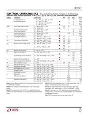
The ● denotes the specifications which apply over the full operating
temperature range, otherwise specifications are at T
A
= 25°C. V
CM
= 0, ±5V ≤ V
S
≤ ±15V, pulse tested, unless otherwise noted.
SYMBOL PARAMETER CONDITIONS MIN TYP MAX UNITS
Inverting Input Current V
S
= ±15V, V
CM
= ±13V, T
A
= 25°C 3.5 10 µA/V
Common Mode Rejection V
S
= ±15V, V
CM
= ±12V ● 10 µA/V
V
S
= ±5V, V
CM
= ±3V, T
A
= 25°C 4.5 10 µA/V
V
S
= ±5V, V
CM
= ±2V ● 10 µA/V
PSRR Power Supply Rejection Ratio V
S
= ±2V to ±15V, T
A
= 25°C6080dB
V
S
= ±3V to ±15V ● 60 dB
Noninverting Input Current V
S
= ±2V to ±15V, T
A
= 25°C250nA/V
Power Supply Rejection V
S
= ±3V to ±15V ● 50 nA/V
Inverting Input Current V
S
= ±2V to ±15V, T
A
= 25°C 0.25 5 µA/V
Power Supply Rejection V
S
= ±3V to ±15V ● 5 µA/V
A
V
Large-Signal Voltage Gain V
S
= ±15V, V
OUT
= ±10V, R
L
= 1k ● 55 72 dB
V
S
= ±5V, V
OUT
= ±2V, R
L
= 150Ω ● 55 72 dB
R
OL
Transresistance, ∆V
OUT
/∆I
IN
– V
S
= ±15V, V
OUT
= ±10V, R
L
= 1k ● 100 270 kΩ
V
S
= ±5V, V
OUT
= ±2V, R
L
= 150Ω ● 100 240 kΩ
V
OUT
Maximum Output Voltage Swing V
S
= ±15V, R
L
= 400Ω, T
A
= 25°C ±12 ±13.5 V
● ±10 V
V
S
= ±5V, R
L
= 150Ω, T
A
= 25°C ±3 ±3.7 V
● ±2.5 V
I
OUT
Maximum Output Current R
L
= 0Ω, T
A
= 25°C3060mA
I
S
Supply Current (Note 3) V
S
= ±15V, V
OUT
= 0V, T
A
= 25°C 10 15.0 mA
● 17.5 mA
Positive Supply Current, Shutdown V
S
= ±15V, Pin 8 Voltage = 0V, T
A
= 25°C 120 300 µA
● 500 µA
I
8
Shutdown Pin Current (Note 4) V
S
= ±15V ● 300 µA
Output Leakage Current, Shutdown V
S
= ±15V, Pin 8 Voltage = 0V, T
A
= 25°C10µA
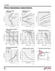
SR Slew Rate (Notes 5 and 6) T
A
= 25°C 500 1100 V/µs
t
r
, t
f
Rise and Fall Time, V
OUT
= 1V
P-P
V
S
= ±5V, R
F
= 1k, R
G
= 1k, R
L
= 150Ω 8.7 ns
BW Small-Signal Bandwidth V
S
= ±15V, R
F
= 1k, R
G
= 1k, R
L
= 150Ω 140 MHz
t
r
, t
f
Small-Signal Rise and Fall Time V
S
= ±15V, R
F
= 1k, R
G
= 1k, R
L
= 100Ω 3.3 ns
Propagation Delay V
S
= ±15V, R
F
= 1k, R
G
= 1k, R
L
= 100Ω 3.4 ns
Small-Signal Overshoot V
S
= ±15V, R
F
= 1k, R
G
= 1k, R
L
= 100Ω 5%
t
S
Settling Time 0.1%, V
OUT
= 10V, R
F
= 1k, R
G
= 1k, R
L
= 1k 50 ns
Differential Gain (Note 7) V
S
= ±15V, R
F
= 1k, R
G
= 1k, R
L
= 150Ω 0.014 %
V
S
= ±15V, R
F
= 1k, R
G
= 1k, R
L
= 1k 0.010 %
Differential Phase (Note 7) V
S
= ±15V, R
F
= 1k, R
G
= 1k, R
L
= 150Ω 0.010 DEG
V
S
= ±15V, R
F
= 1k, R
G
= 1k, R
L
= 1k 0.013 DEG
Note 1: Absolute Maximum Ratings are those values beyond which the life
of a device may be impaired.
Note 2: A heat sink may be required depending on the power supply
voltage.
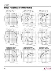
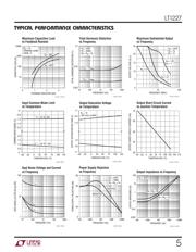
Note 3: The supply current of the LT1227 has a negative temperature
coefficient. For more information, see Typical Performance Characteristics
curves.
Note 4: Ramp Pin 8 voltage down from 15V while measuring I
S
. When I
S
drops to less than 0.5mA, measure Pin 8 current.
Note 5: Slew rate is measured at ±5V on a ±10V output signal while
operating on ±15V supplies with R
F
= 2k, R
G
= 220Ω and R
L
= 400Ω.
Note 6: AC parameters are 100% tested on the ceramic and plastic DIP
package parts (J and N suffix) and are sample tested on every lot of the SO
packaged parts (S suffix).
Note 7: NTSC composite video with an output level of 2V.
器件 Datasheet 文档搜索
AiEMA 数据库涵盖高达 72,405,303 个元件的数据手册,每天更新 5,000 多个 PDF 文件
