Datasheet 搜索 > 运算放大器 > Linear Technology(凌力尔特) > LT1355CN8#PBF 数据手册 > LT1355CN8#PBF 数据手册 6/17 页
 器件3D模型
¥ 38.326
LT1355CN8#PBF 数据手册 - Linear Technology(凌力尔特)
制造商:
Linear Technology(凌力尔特)
分类:
运算放大器
封装:
DIP-8
描述:
LINEAR TECHNOLOGY LT1355CN8#PBF 运算放大器, 双路, 12 MHz, 2个放大器, 400 V/µs, ± 2.5V 至 ± 15V, DIP, 8 引脚
Pictures:
3D模型
符号图
焊盘图
引脚图
产品图
页面导航:
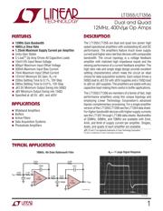
典型应用电路图在P17
技术参数、封装参数在P6
应用领域在P6P10P11P12P17
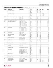
电气规格在P4P5P6P7P8P9P10

导航目录
LT1355CN8#PBF数据手册
Page:
of 17 Go
若手册格式错乱,请下载阅览PDF原文件
5
LT1355/LT1356
SYMBOL PARAMETER CONDITIONS V
SUPPLY
MIN TYP MAX UNITS
ELECTRICAL CHARACTERISTICS
V
OUT
= ±2.5V, R
L
= 150Ω±5V ● 0.4 V/mV
V
OUT
= ±1V, R
L
= 500Ω±2.5V ● 1.7 V/mV
V
OUT
Output Swing R
L
= 1k, V
IN
= ±40mV ±15V ● 13.0 ±V
R
L
= 500Ω, V
IN
= ±40mV ±15V ● 11.5 ±V
R
L
= 500Ω, V
IN
= ±40mV ±5V ● 3.4 ±V
R
L
= 150Ω, V
IN
= ±40mV ±5V ● 2.6 ±V
R
L
= 500Ω, V
IN
= ±40mV ±2.5V ● 1.2 ±V
I
OUT
Output Current V
OUT
= ±11.5V ±15V ● 23.0 mA
V
OUT
= ±2.6V ±5V ● 17.3 mA
I
SC
Short-Circuit Current V
OUT
= 0V, V
IN
= ±3V ±15V ● 23 mA
SR Slew Rate A
V
= –2, (Note 4) ±15V ● 120 V/µs
±5V
● 50 V/µs
GBW Gain Bandwidth f = 200kHz, R
L
= 2k ±15V ● 7.0 MHz
±5V
● 5.5 MHz
Channel Separation V
OUT
= ±10V, R
L
= 500Ω±15V ● 98 dB
I
S
Supply Current Each Amplifier ±15V ● 1.50 mA
Each Amplifier ±5V ● 1.45 mA
Note 1: Absolute Maximum Ratings are those values beyond which the life
of a device may be impaired.
Note 2: Differential inputs of ±10V are appropriate for transient operation
only, such as during slewing. Large, sustained differential inputs will cause
excessive power dissipation and may damage the part. See Input
Considerations in the Applications Information section of this data sheet
for more details.
Note 3: A heat sink may be required to keep the junction temperature
below absolute maximum when the output is shorted indefinitely.
Note 4: Slew rate is measured between ±10V on the output with ±6V input
for ±15V supplies and ±1V on the output with ±1.75V input for ±5V
supplies.
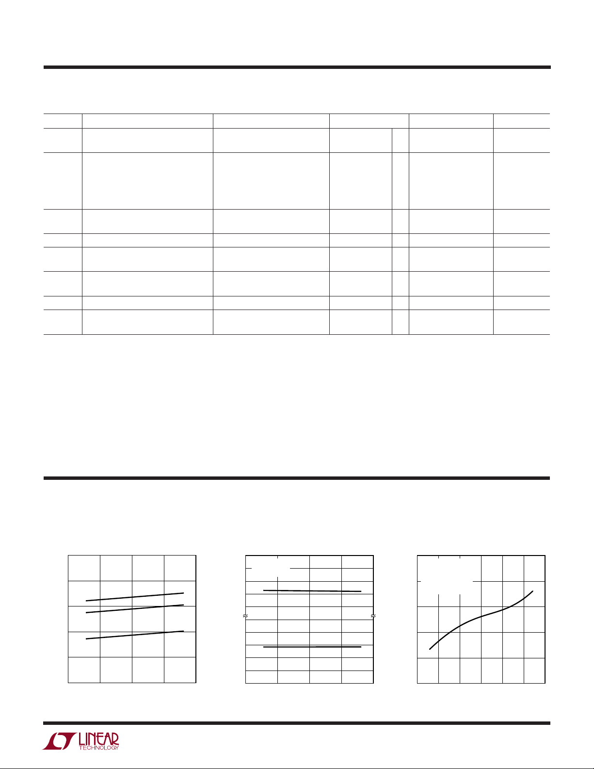
TYPICAL PERFORMANCE CHARACTERISTICS
U
W
Input Common Mode Range vs
Supply Voltage
Supply Current vs Supply Voltage
and Temperature
SUPPLY VOLTAGE (±V)
V
–
COMMON MODE RANGE (V)
2.0
0.5
1.0
1.5
V
+
–1.0
–0.5
–2.0
–1.5
10501520
1355/1356 G02
T
A
= 25°C
∆V
OS
< 1mV
Input Bias Current vs
Input Common Mode Voltage
INPUT COMMON MODE VOLTAGE (V)
–50
INPUT BIAS CURRENT (nA)
0
200
150
100
50
–15 –10 0 10 155–5
1355/1356 G03
V
S
= ±15V
T
A
= 25°C
I
B
=
I
B
+
+ I
B
–
————
2
Note 5: Full power bandwidth is calculated from the slew rate
measurement: FPBW = (SR)/2πV
P
.
Note 6: This parameter is not 100% tested.
Note 7: The LT1355C/LT1356C are guaranteed functional over the
operating temperature range of –40°C to 85°C.
Note 8: The LT1355C/LT1356C are guaranteed to meet specified
performance from 0°C to 70°C. The LT1355C/LT1356C are designed,
characterized and expected to meet specified performance from –40°C to
85°C, but are not tested or QA sampled at these temperatures. For
guaranteed I-grade parts, consult the factory.
The ● denotes the specifications which apply over the temperature range
–40°C ≤ T
A
≤ 85°C, V
CM
= 0V unless otherwise noted. (Note 8)
SUPPLY VOLTAGE (±V)
0.4
SUPPLY CURRENT (mA)
0.8
0.6
1.4
1.2
1.0
10501520
1355/1356 G01
–55°C
25°C
125°C
器件 Datasheet 文档搜索
AiEMA 数据库涵盖高达 72,405,303 个元件的数据手册,每天更新 5,000 多个 PDF 文件
