Datasheet 搜索 > DC/DC转换器 > Linear Technology(凌力尔特) > LT1372CN8#PBF 数据手册 > LT1372CN8#PBF 数据手册 10/12 页
 器件3D模型
¥ 35.204
LT1372CN8#PBF 数据手册 - Linear Technology(凌力尔特)
制造商:
Linear Technology(凌力尔特)
分类:
DC/DC转换器
封装:
DIP-8
描述:
Linear Technology 的各种高效直流 - 直流转换器可作为升压(增压)调节器、降压(减压)调节器或反相调节器。 这些高度集成设备只需极少的外部元件,即可提供全面的调节器功能和多种组合功能,如微功耗操作、低电量检测、可调电流限制以及关闭/启用输入。### 开关电压调节器,Linear Technology**Linear Technology** 的同步型和非同步型内部开关调节器 IC 产品系列效率高、输入电压范围广、且开关频率高达 4 MHz。 该系列控制器包括多种配置:从降压(下降),升压(上压)、降压-升压、正向、隔离、反相和反激控制器。 反激、正向和隔离控制器(一次侧和二次侧)提供解决方案,帮助更换背板型电源转换中使用的直流/直流砖型转换器。
Pictures:
3D模型
符号图
焊盘图
引脚图
产品图
页面导航:
典型应用电路图在P7P11P12
技术参数、封装参数在P3
应用领域在P5P7P11P12
电气规格在P3
导航目录
LT1372CN8#PBF数据手册
Page:
of 12 Go
若手册格式错乱,请下载阅览PDF原文件
10
LT1372/LT1377
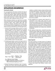
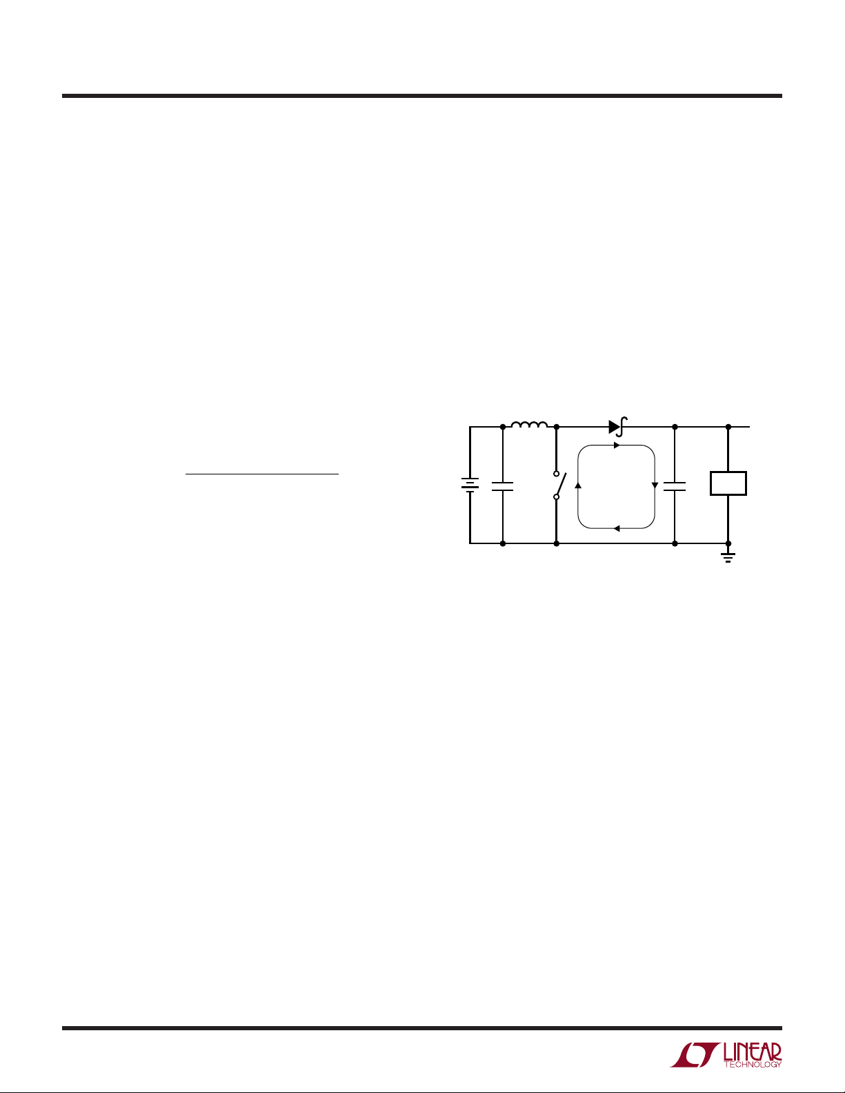
(magnetic) radiation is minimized by keeping output di-
ode, switch pin, and output bypass capacitor leads as
short as possible. E field radiation is kept low by minimiz-
ing the length and area of all traces connected to the switch
pin. A ground plane should always be used under the
switcher circuitry to prevent interplane coupling.
The high speed switching current path is shown schemati-
cally in Figure 3. Minimum lead length in this path is
essential to ensure clean switching and low EMI. The path
including the switch, output diode, and output capacitor is
the only one containing nanosecond rise and fall times.
Keep this path as short as possible.
LOAD
V
OUT
L1
SWITCH
NODE
LT1372 • F03
V
IN
HIGH
FREQUENCY
CIRCULATING
PATH
Figure 3
More Help
For more detailed information on switching regulator
circuits, please see Application Note 19. Linear Technol-
ogy also offers a computer software program, SwitcherCAD,
to assist in designing switching converters. In addition,
our applications department is always ready to lend a
helping hand.
Frequency Compensation
Loop frequency compensation is performed on the output
of the error amplifier (V
C
pin) with a series RC network.
The main pole is formed by the series capacitor and the
output impedance (≈500kΩ) of the error amplifier. The
pole falls in the range of 2Hz to 20Hz. The series resistor
creates a “zero” at 1kHz to 5kHz, which improves loop
stability and transient response. A second capacitor,
typically one-tenth the size of the main compensation
capacitor, is sometimes used to reduce the switching
frequency ripple on the V
C
pin. V
C
pin ripple is caused by
output voltage ripple attenuated by the output divider and
multiplied by the error amplifier. Without the second
capacitor, V
C
pin ripple is:
V
C
Pin Ripple =
V
RIPPLE
= Output ripple (V
P–P
)
g
m
= Error amplifier transconductance
(≈1500µmho)
R
C
= Series resistor on V
C
pin
V
OUT
= DC output voltage
1.245(V
RIPPLE
)(g
m
)(R
C
)
(V
OUT
)
To prevent irregular switching, V
C
pin ripple should be
kept below 50mV
P–P
.
Worst-case V
C
pin ripple occurs at
maximum output load current and will also be increased
if poor quality (high ESR) output capacitors are used. The
addition of a 0.0047µF capacitor on the V
C
pin reduces
switching frequency ripple to only a few millivolts. A low
value for R
C
will also reduce V
C
pin ripple, but loop phase
margin may be inadequate.
Switch Node Considerations
For maximum efficiency, switch rise and fall time are
made as short as possible. To prevent radiation and high
frequency resonance problems, proper layout of the com-
ponents connected to the switch node is essential. B field
APPLICATIO S I FOR ATIO
WUUU
器件 Datasheet 文档搜索
AiEMA 数据库涵盖高达 72,405,303 个元件的数据手册,每天更新 5,000 多个 PDF 文件
