Datasheet 搜索 > ADI(亚德诺) > LT1372CS8#PBF 数据手册 > LT1372CS8#PBF 数据手册 7/12 页
 器件3D模型
¥ 23.697
LT1372CS8#PBF 数据手册 - ADI(亚德诺)
制造商:
ADI(亚德诺)
封装:
SOIC-8
描述:
降压型 升降压型 升压型 Vin=2.7V~30V Vout=1.245V~35V 1.5A
Pictures:
3D模型
符号图
焊盘图
引脚图
产品图
页面导航:
典型应用电路图在P7P11P12
技术参数、封装参数在P3
应用领域在P5P7P11P12
电气规格在P3
导航目录
LT1372CS8#PBF数据手册
Page:
of 12 Go
若手册格式错乱,请下载阅览PDF原文件
7
LT1372/LT1377
Positive fixed voltage versions are available (consult
Linear Technology marketing).
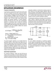
Negative Output Voltage Setting
The LT1372/LT1377 develops a –2.49V reference (V
NFR
)
from the NFB pin to ground. Output voltage is set by
connecting the NFB pin to an output resistor divider
(Figure 2). The –30µA NFB pin bias current (I
NFB
) can
cause output voltage errors and should not be ignored.
This has been accounted for in the formula in Figure 2. The
suggested value for R2 is 2.49k. The FB pin is normally left
open for negative output application. See Dual Polarity
Output Voltage Sensing for limitatins on FB pin loading
when using the NFB pin.
Shutdown and Synchronization
The dual function S/S pin provides easy shutdown and
synchronization. It is logic level compatible and can be
pulled high, tied to V
IN
or left floating for normal operation.
A logic low on the S/S pin activates shutdown, reducing
the part’s supply current to 12µA. Typical synchronization
range is from 1.05 to 1.8 times the part’s natural switching
frequency, but is only guaranteed between 600kHz and
800kHz (LT1372) or 1.2MHz and 1.6MHz (LT1377). At
start-up, the synchronization signal should not be applied
until the feedback pin is above the frequency shift voltage
of 0.7V. If the NFB pin is used, synchronization should not
be applied until the NFB pin is more negative than –1.4V.
A 12µs resetable shutdown delay network guarantees the
part will not go into shutdown while receiving a synchro-
nization signal.
Caution should be used when synchronizing above 700kHz
(LT1372) or 1.4MHz (LT1377) because at higher sync
frequencies the amplitude of the internal slope compensa-
tion used to prevent subharmonic switching is reduced.
This type of subharmonic switching only occurs when the
duty cycle of the switch is above 50%. Higher inductor
values will tend to eliminate problems.
Thermal Considerations
Care should be taken to ensure that the worst-case input
voltage and load current conditions do not cause exces-
sive die temperatures. The packages are rated at 120°C/W
for SO (S8) and 130°C/W for PDIP (N8).
Average supply current (including driver current) is:
I
IN
= 4mA + DC (I
SW
/60 + I
SW
× 0.004)
I
SW
= switch current
DC = switch duty cycle
Switch power dissipation is given by:
P
SW
= (I
SW
)
2
× R
SW
× DC
R
SW
= output switch “On” resistance
Total power dissipation of the die is the sum of supply
current times supply voltage plus switch power:
P
D(TOTAL)
= (I
IN
× V
IN
) + P
SW
Dual Polarity Output Voltage Sensing
Certain applications benefit from sensing both positive
and negative output voltages. One example is the “Dual
Output Flyback Converter with Overvoltage Protection”
circuit shown in the Typical Applications section. Each
output voltage resistor divider is individually set as de-
scribed above. When both the FB and NFB pins are used,
the LT1372/LT1377 acts to prevent either output from
going beyond its set output voltage. For example in this
application, if the positive output were more heavily loaded
than the negative, the negative output would be greater
and would regulate at the desired set-point voltage. The
positive output would sag slightly below its set-point
voltage. This technique prevents either output from going
unregulated high at no load. Please note that the load on
the FB pin should not exceed 250µA when the NFB pin is
used. This situation occurs when the resistor dividers are
used at
both
FB and NFB. True load on FB is not the full
divider current unless the positive output is shorted to
ground. See Dual Output Flyback Converter application.
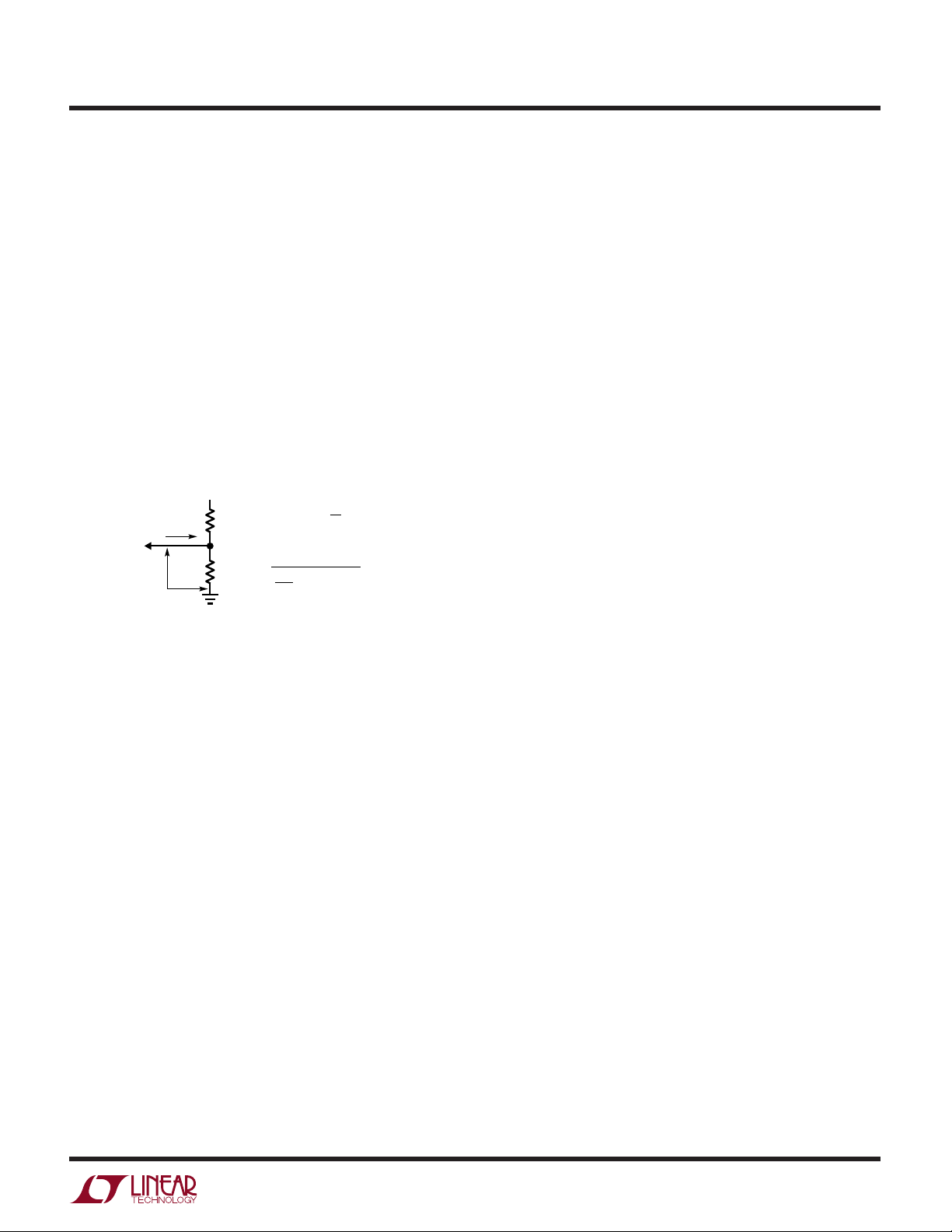
R1
–V
OUT
= V
NFB
+ I
NFB
(R1)1 +
R2
LT1372 • F02
NFB
PIN
V
NFR
I
NFB
–V
OUT
()
R1
R2
R1 =
+ 30 × 10
–
6
V
OUT
– 2.49
( ) ( )
2.49
R2
Figure 2. Negative Output Resistor Divider
APPLICATIO S I FOR ATIO
WUUU
器件 Datasheet 文档搜索
AiEMA 数据库涵盖高达 72,405,303 个元件的数据手册,每天更新 5,000 多个 PDF 文件
