Datasheet 搜索 > DC/DC转换器 > Linear Technology(凌力尔特) > LT1372CS8#TR 数据手册 > LT1372CS8#TR 数据手册 5/12 页
 器件3D模型
¥ 29.051
LT1372CS8#TR 数据手册 - Linear Technology(凌力尔特)
制造商:
Linear Technology(凌力尔特)
分类:
DC/DC转换器
封装:
SO
Pictures:
3D模型
符号图
焊盘图
引脚图
产品图
页面导航:
典型应用电路图在P7P11P12
技术参数、封装参数在P3
应用领域在P5P7P11P12
电气规格在P3
导航目录
LT1372CS8#TR数据手册
Page:
of 12 Go
若手册格式错乱,请下载阅览PDF原文件
5
LT1372/LT1377
V
C
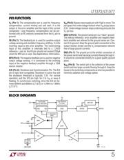
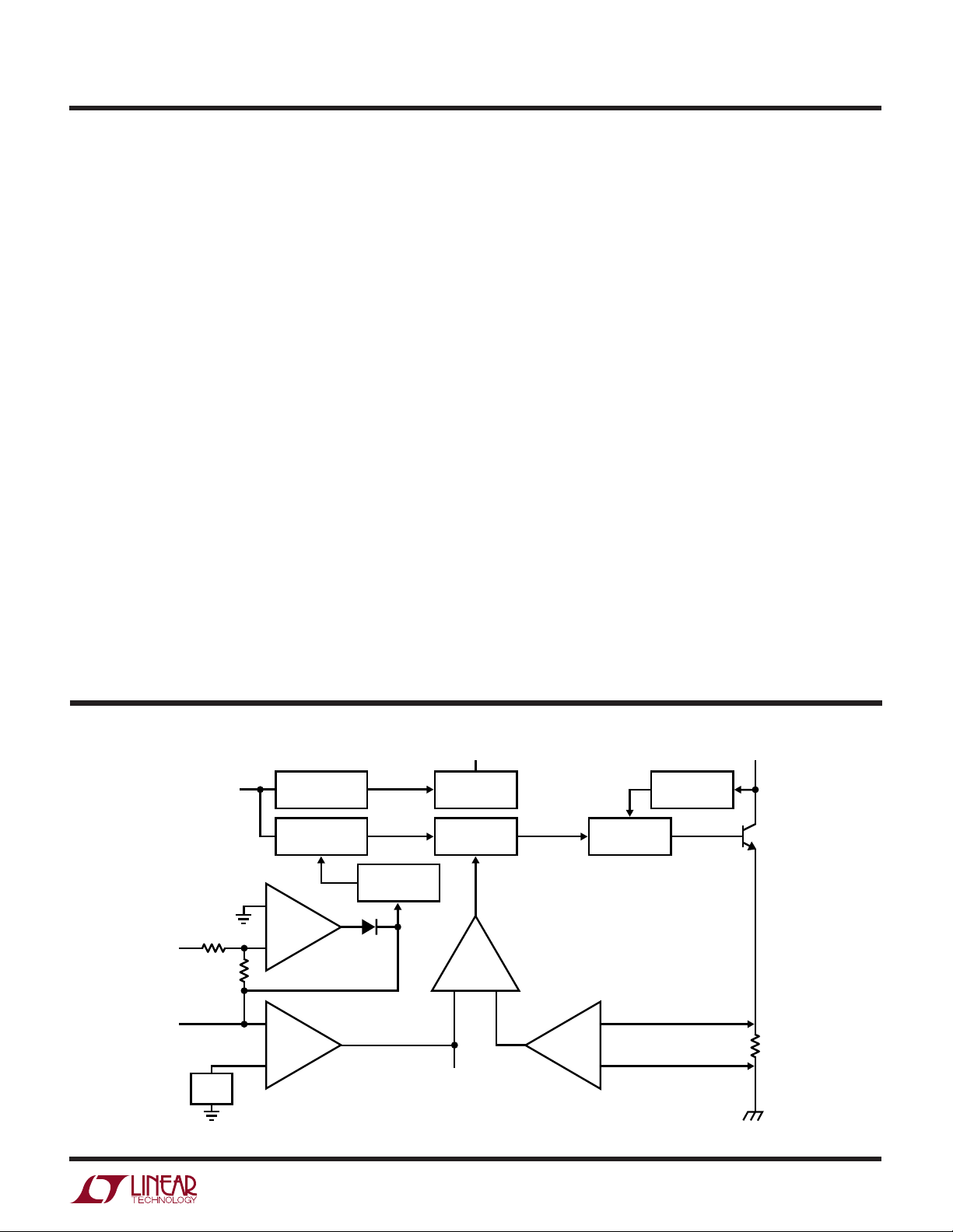
(Pin 1): The compensation pin is used for frequency
compensation, current limiting and soft start. It is the
output of the error amplifier and the input of the current
comparator. Loop frequency compensation can be per-
formed with an RC network connected from the V
C
pin to
ground.
FB (Pin 2): T
he feedback pin is used for positive output
voltage sensing and oscillator frequency shifting. It is the
inverting input to the error amplifier. The noninverting
input of this amplifier is internally tied to a 1.245V
reference. Load on the FB pin should not exceed 250µA
when the NFB pin is used. See Applications Information.
NFB (Pin 3): The negative feedback pin is used for negative
output voltage sensing. It is connected to the inverting
input of the negative feedback amplifier through a 100k
source resistor.
S/S (Pin 4): Shutdown and Synchronization Pin. The S/S
pin is logic level compatible. Shutdown is active low and
the shutdown threshold is typically 1.3V. For normal
operation, pull the S/S pin high, tie it to V
IN
or leave it
floating. To synchronize switching, drive the S/S pin be-
tween 600kHz and 800kHz (LT1372) or 1.2MHz to 1.6MHz
(LT1377).
V
IN
(Pin 5): Bypass input supply pin with 10µF or more. The
part goes into undervoltage lockout when V
IN
drops below
2.5V. Undervoltage lockout stops switching and pulls the
V
C
pin low.
GND S (Pin 6): The ground sense pin is a “clean” ground.
The internal reference, error amplifier and negative feed-
back amplifier are referred to the ground sense pin. Con-
nect it to ground. Keep the ground path connection to the
output resistor divider and the V
C
compensation network
free of large ground currents.
GND (Pin 7): The ground pin is the emitter connection of
the power switch and has large currents flowing through it.
It should be connected directly to a good quality ground
plane.
V
SW
(Pin 8): The switch pin is the collector of the power
switch and has large currents flowing through it. Keep the
traces to the switching components as short as possible to
minimize radiation and voltage spikes.
–
+
NFBA
NFB
S/S
FB
100k
50k
0.08Ω
–
+
EA
V
C
V
IN
GND LT1372 • BD
GND SENSE
1.245V
REF
5:1 FREQUENCY
SHIFT
OSCSYNC
SHUTDOWN
DELAY AND RESET
LOW DROPOUT
2.3V REG
ANTI-SAT
LOGIC DRIVER
SW
SWITCH
–
+
IA
A
V
≈ 6
COMP
UU
U
PI FU CTIO S
BLOCK DIAGRA
W
器件 Datasheet 文档搜索
AiEMA 数据库涵盖高达 72,405,303 个元件的数据手册,每天更新 5,000 多个 PDF 文件
