Datasheet 搜索 > ADI(亚德诺) > LT1376HVIS8 数据手册 > LT1376HVIS8 数据手册 6/28 页

 器件3D模型
¥ 19.964
LT1376HVIS8 数据手册 - ADI(亚德诺)
制造商:
ADI(亚德诺)
封装:
SOP
Pictures:
3D模型
符号图
焊盘图
引脚图
产品图
页面导航:
引脚图在P6P7P8P16Hot
原理图在P7P8
焊盘布局在P27P28
技术参数、封装参数在P4
应用领域在P1P4P5P7P8P9P10P11P12P13P14P15
电气规格在P3P4P5P6P10P11P24
导航目录
LT1376HVIS8数据手册
Page:
of 28 Go
若手册格式错乱,请下载阅览PDF原文件
6
LT1375/LT1376
13756fd
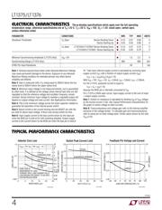
TYPICAL PERFORMANCE CHARACTERISTICS
U
W
INPUT VOLTAGE (V)
0
CURRENT (A)
1.50
1.25
1.00
0.75
0.50
0.25
0
5101520
1375/76 G13
25
L = 20µH
L = 10µH
L = 5µH
V
OUT
= 10V
INPUT VOLTAGE (V)
0
CURRENT (A)
1.50
1.25
1.00
0.75
0.50
0.25
0
5101520
1375/76 G14
25
L = 20µH
L = 10µH
L = 5µH
V
OUT
= 3.3V
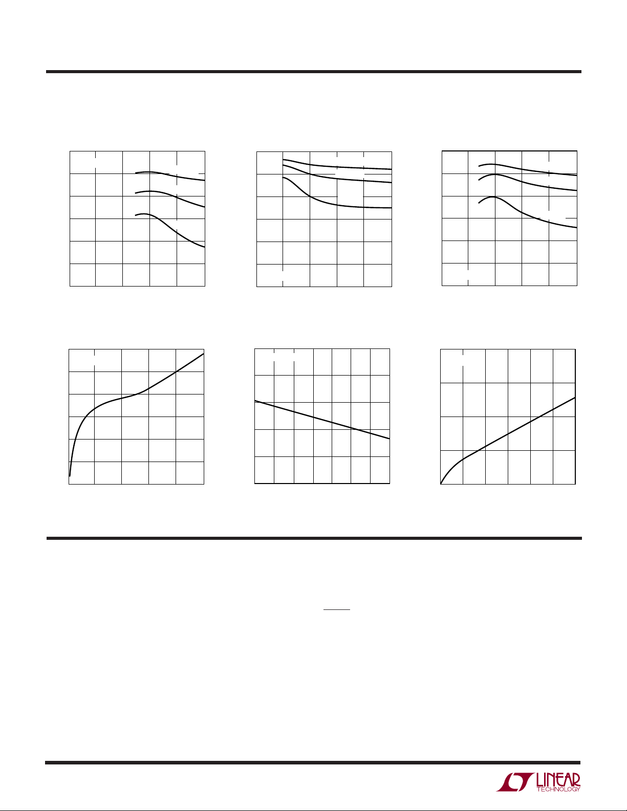
Maximum Load Current
at V
OUT
= 10V
Maximum Load Current
at V
OUT
= 3.3V
Maximum Load Current
at V
OUT
= 5V
INPUT VOLTAGE (V)
0
CURRENT (A)
1.50
1.25
1.00
0.75
0.50
0.25
0
5101520
1375/76 G15
25
L = 20µH
L = 10µH
L = 5µH
V
OUT
= 5V
PIN FUNCTIONS
UUU
BOOST: The BOOST pin is used to provide a drive voltage,
higher than the input voltage, to the internal bipolar NPN
power switch. Without this added voltage, the typical
switch voltage loss would be about 1.5V. The additional
boost voltage allows the switch to saturate and voltage
loss approximates that of a 0.3Ω FET structure, but with
much smaller die area. Efficiency improves from 75% for
conventional bipolar designs to > 87% for these new parts.
V
SW
: The switch pin is the emitter of the on-chip power
NPN switch. It is driven up to the input pin voltage during
switch on time. Inductor current drives the switch pin
negative during switch off time. Negative voltage is clamped
with the external catch diode. Maximum negative switch
voltage allowed is –0.8V.
SHDN: The shutdown pin is used to turn off the regulator
and to reduce input drain current to a few microamperes.
Actually, this pin has two separate thresholds, one at
2.38V to disable switching, and a second at 0.4V to force
complete micropower shutdown. The 2.38V threshold
functions as an accurate undervoltage lockout (UVLO).
This is sometimes used to prevent the regulator from
operating until the input voltage has reached a predeter-
mined level.
SWITCH CURRENT (A)
0
BOOST PIN CURRENT (mA)
12
10
8
6
4
2
0
0.25 0.50 0.75 1.00
1375/76 G16
1.25
T
J
= 25°C
BOOST Pin Current
V
C
Pin Shutdown Threshold
SWITCH CURRENT (A)
0
SWITCH VOLTAGE (V)
0.8
0.6
0.4
0.2
0
0.25 0.50 0.75 1.00
1375/76 G18
1.25 1.50
T
J
= 25°C
Switch Voltage Drop
JUNCTION TEMPERATURE (°C)
–50
1.4
1.2
1.0
0.8
0.6
0.4
100
1375/76 G11
–25 0 25 50 75 125
THRESHOLD VOLTAGE (V)
SHUTDOWN
器件 Datasheet 文档搜索
AiEMA 数据库涵盖高达 72,405,303 个元件的数据手册,每天更新 5,000 多个 PDF 文件
