Datasheet 搜索 > 电压基准芯片 > Linear Technology(凌力尔特) > LT1461BIS8-4#PBF 数据手册 > LT1461BIS8-4#PBF 数据手册 3/16 页
 器件3D模型
¥ 35.879
LT1461BIS8-4#PBF 数据手册 - Linear Technology(凌力尔特)
制造商:
Linear Technology(凌力尔特)
分类:
电压基准芯片
封装:
SOIC-8
描述:
LINEAR TECHNOLOGY LT1461BIS8-4#PBF 电压基准, 精准微功率, 低压降, 系列 - 固定, LT1461系列, 4.096V, NSOIC-8
Pictures:
3D模型
符号图
焊盘图
引脚图
产品图
页面导航:
技术参数、封装参数在P3
应用领域在P3P4P9
电气规格在P3P4P5P6P7P8P9P12
导航目录
LT1461BIS8-4#PBF数据手册
Page:
of 16 Go
若手册格式错乱,请下载阅览PDF原文件
3
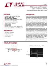
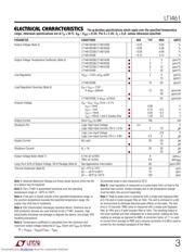
LT1461
PARAMETER CONDITIONS MIN TYP MAX UNITS
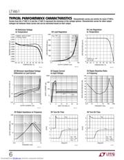
Output Voltage (Note 4) LT1461ACS8/LT1461AIS8 –0.04 0.04 %
LT1461BCS8/LT1461BIS8 –0.06 0.06 %
LT1461CCS8/LT1461CIS8 –0.08 0.08 %
LT1461DHS8 –0.15 0.15 %
Output Voltage Temperature Coefficient (Note 5) LT1461ACS8/LT1461AIS8 ● 1 3 ppm/°C
LT1461BCS8/LT1461BIS8
● 3 7 ppm/°C
LT1461CCS8/LT1461CIS8
● 5 12 ppm/°C
LT1461DHS8
● 7 20 ppm/°C
Line Regulation (V
OUT
+ 0.5V) ≤ V
IN
≤ 20V 2 8 ppm/V
● 12 ppm/V
LT1461DHS8 ● 15 50 ppm/V
Load Regulation Sourcing (Note 6) V
IN
= V
OUT
+ 2.5V
0 ≤ I
OUT
≤ 50mA 12 30 ppm/mA
● 40 ppm/mA
LT1461DHS8, 0 ≤ I
OUT
≤ 10mA ● 50 ppm/mA
Dropout Voltage V
IN
– V
OUT
, V
OUT
Error = 0.1%
I
OUT
= 0mA 0.06 V
I
OUT
= 1mA ● 0.13 0.3 V
I
OUT
= 10mA ● 0.20 0.4 V
I
OUT
= 50mA, I and C Grades Only ● 1.50 2.0 V
Output Current Short V
OUT
to GND 100 mA
Shutdown Pin Logic High Input Voltage ● 2.4 V
Logic High Input Current, Pin 3 = 2.4V
● 215 µA
Logic Low Input Voltage ● 0.8 V
Logic Low Input Current, Pin 3 = 0.8V
● 0.5 4 µA
Supply Current No Load 35 50 µA
● 70 µA
Shutdown Current R
L
= 1k 25 35 µA
● 55 µA
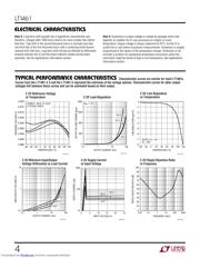
Output Voltage Noise (Note 7) 0.1Hz ≤ f ≤ 10Hz 8 ppm
P-P
10Hz ≤ f ≤ 1kHz 9.6 ppm
RMS
Long-Term Drift of Output Voltage, SO-8 Package (Note 8) See Applications Information 60 ppm/√kHr
Thermal Hysteresis (Note 9) ∆T = 0°C to 70°C 40 ppm
∆T = –40°C to 85°C 75 ppm
∆T = –40°C to 125°C 120 ppm
The ● denotes specifications which apply over the specified temperature
range, otherwise specifications are at T
A
= 25°C. V
IN
– V
OUT
= 0.5V, Pin 3 = 2.4V, C
L
= 2µF, unless otherwise specified.
ELECTRICAL CHARACTERISTICS
Note 1: Absolute Maximum Ratings are those values beyond which the life
of a device may be impaired.
Note 2: The LT1461 is guaranteed functional over the operating
temperature range of –40°C to 125°C.
Note 3: If the part is stored outside of the specified temperature range, or
the junction temperature exceeds the specified temperature range, the
output may shift due to hysteresis.
Note 4: ESD (Electrostatic Discharge) sensitive device. Extensive use of
ESD protection devices are used internal to the LT1461, however, high
electrostatic discharge can damage or degrade the device. Use proper ESD
handling precautions.
Note 5: Temperature coefficient is calculated from the minimum and
maximum output voltage measured at T
MIN
, Room and T
MAX
as follows:
TC = (V
OMAX
– V
OMIN
)/(T
MAX
– T
MIN
)
Incremental slope is also measured at 25°C.
Note 6: Load regulation is measured on a pulse basis from no load to the
specified load current. Output changes due to die temperature change
must be taken into account separately.
Note 7: Peak-to-peak noise is measured with a single pole highpass filter
at 0.1Hz and a 2-pole lowpass filter at 10Hz. The unit is enclosed in a still-
air environment to eliminate thermocouple effects on the leads. The test
time is 10 seconds. RMS noise is measured with a single pole highpass
filter at 10Hz and a 2-pole lowpass filter at 1kHz. The resulting output is
full-wave rectified and then integrated for a fixed period, making the final
reading an average as opposed to RMS. A correction factor of 1.1 is used
to convert from average to RMS and a second correction of 0.88 is used to
correct for the nonideal bandpass of the filters.
Downloaded from Elcodis.com electronic components distributor
器件 Datasheet 文档搜索
AiEMA 数据库涵盖高达 72,405,303 个元件的数据手册,每天更新 5,000 多个 PDF 文件
