Datasheet 搜索 > 放大器、缓冲器 > Linear Technology(凌力尔特) > LT1806IS8#TRPBF 数据手册 > LT1806IS8#TRPBF 数据手册 1/28 页
 器件3D模型
¥ 20.484
LT1806IS8#TRPBF 数据手册 - Linear Technology(凌力尔特)
制造商:
Linear Technology(凌力尔特)
分类:
放大器、缓冲器
封装:
SOIC-8
Pictures:
3D模型
符号图
焊盘图
引脚图
产品图
页面导航:
典型应用电路图在P1P21P22P23P24P28
原理图在P17
封装尺寸在P27
焊盘布局在P25P26P27
技术参数、封装参数在P11
应用领域在P1P11P17P18P19P20P21P22P23P24
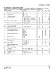
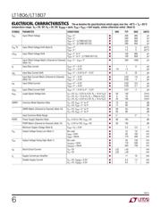
电气规格在P3P4P5P6P7P8P9P10P11P12P13P14
导航目录
LT1806IS8#TRPBF数据手册
Page:
of 28 Go
若手册格式错乱,请下载阅览PDF原文件
LT1806/LT1807
1
18067fc
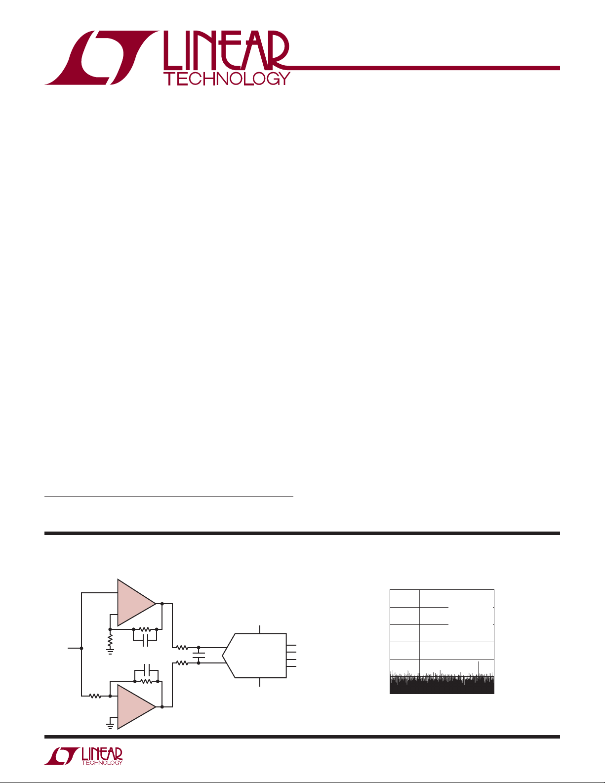
TYPICAL APPLICATION
DESCRIPTION
325MHz, Single/Dual,
Rail-to-Rail Input and Output, Low Distortion,
Low Noise Precision Op Amps
The LT
®
1806/LT1807 are single/dual low noise rail-to-rail
input and output unity-gain stable op amps that feature a
325MHz gain-bandwidth product, a 140V/μs slew rate and
a 85mA output current. They are optimized for low voltage,
high performance signal conditioning systems.
The LT1806/LT1807 have a very low distortion of – 80dBc
at 5MHz, a low input referred noise voltage of 3.5nV/√Hz
and a maximum offset voltage of 550μV that allows them to
be used in high performance data acquisition systems.
The LT1806/LT1807 have an input range that includes
both supply rails and an output that swings within 20mV
of either supply rail to maximize the signal dynamic range
in low supply applications.
The LT1806/LT1807 maintain their performance for supplies
from 2.5V to 12.6V and are specifi ed at 3V, 5V and ±5V
supplies. The inputs can be driven beyond the supplies
without damage or phase reversal of the output.
The LT1806 is available in an 8-pin SO package with the
standard op amp pinout and a 6-pin TSOT-23 package. The
LT1807 features the standard dual op amp pinout and is
available in 8-pin SO and MSOP packages.These devices
can be used as plug-in replacements for many op amps
to improve input/output range and performance.
FEATURES
APPLICATIONS
n
Low Voltage, High Frequency Signal Processing
n
Driving A/D Converters
n
Rail-to-Rail Buffer Amplifi ers
n
Active Filters
n
Video Line Driver
n
Gain-Bandwidth Product: 325MHz
n
Slew Rate: 140V/μs
n
Wide Supply Range: 2.5V to 12.6V
n
Large Output Current: 85mA
n
Low Distortion, 5MHz: –80dBc
n
Low Voltage Noise: 3.5nV/√Hz
n
Input Common Mode Range Includes Both Rails
n
Output Swings Rail-to-Rail
n
Input Offset Voltage (Rail-to-Rail): 550μV Max
n
Common Mode Rejection: 106dB Typ
n
Power Supply Rejection: 105dB Typ
n
Unity-Gain Stable
n
Power Down Pin (LT1806)
n
Operating Temperature Range: –40°C to 85°C
n
Single in SO-8 and 6-Pin Low Profi le (1mm)
ThinSOT™ Packages
n
Dual in SO-8 and 8-Pin MSOP Packages
–
+
1/2 LT1807
R2
909Ω
R5
49.9Ω
R6
49.9Ω
R3
100Ω
V
IN
R1
100Ω
C1 5.6pF
C2 5.6pF
–
+
1/2 LT1807
R4
1k
C3
470pF
LT C
®
1420
PGA GAIN = 1
V
REF
= 4.096V
12 BITS
10Msps
+AV
IN
5V
–5V
18067 TA01
–AV
IN
Gain of 20 Differential A/D Driver
FREQUENCY (MHz)
0
–120
AMPLITUDE (dB)
–100
–80
–60
–40
–20
0
1234
18067 TA02
5
V
S
= p5V
A
V
= 20
f
SAMPLE
= 10Msps
f
IN
= 1.4086MHz
SFDR = 83dB
NONAVERAGED
V
IN
= 200mV
P-P
4096 Point FFT Response
L, LT, LTC, LTM, Linear Technology and the Linear logo are registered trademarks of Linear
Technology Corporation. ThinSOT is a trademark of Linear Technology Corporation. All other
trademarks are the property of their respective owners.
器件 Datasheet 文档搜索
AiEMA 数据库涵盖高达 72,405,303 个元件的数据手册,每天更新 5,000 多个 PDF 文件
