Datasheet 搜索 > ADI(亚德诺) > LT3085MPMS8E#PBF 数据手册 > LT3085MPMS8E#PBF 数据手册 3/28 页


¥ 64.023
LT3085MPMS8E#PBF 数据手册 - ADI(亚德诺)
制造商:
ADI(亚德诺)
封装:
MSOP
Pictures:
3D模型
符号图
焊盘图
引脚图
产品图
页面导航:
引脚图在P7Hot
典型应用电路图在P1P18P19P20P21P22P23P24P28
原理图在P8
封装尺寸在P25
焊盘布局在P26
技术参数、封装参数在P3
应用领域在P1P3P8P9P10P11P12P13P14P15P16P17
电气规格在P3P4P5P6P7P13P15
导航目录
LT3085MPMS8E#PBF数据手册
Page:
of 28 Go
若手册格式错乱,请下载阅览PDF原文件
LT3085
3
3085fb
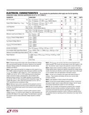
ELECTRICAL CHARACTERISTICS
Note 1: Stresses beyond those listed under Absolute Maximum Ratings
may cause permanent damage to the device. Exposure to any Absolute
Maximum Rating condition for extended periods may affect device
reliability and lifetime.
Note 2. Unless otherwise specifi ed, all voltages are with respect to V
OUT
.
The LT3085 is tested and specifi ed under pulse load conditions such that
T
J
≅ T
A
. The LT3085E is 100% tested at T
A
= 25°C. Performance of the
LT3085E over the full –40°C to 125°C operating junction temperature
range is assured by design, characterization, and correlation with
statistical process controls. The LT3085I regulators are guaranteed
over the full –40°C to 125°C operating junction temperature range. The
LT3085 (MP grade) is 100% tested and guaranteed over the –55°C to
125°C operating junction temperature range.
Note 3. Minimum load current is equivalent to the quiescent current of
the part. Since all quiescent and drive current is delivered to the output
of the part, the minimum load current is the minimum current required to
maintain regulation.
Note 4. For the LT3085, dropout is caused by either minimum control
voltage (V
CONTROL
) or minimum input voltage (V
IN
). Both parameters are
specifi ed with respect to the output voltage. The specifi cations represent
the minimum input-to-output differential voltage required to maintain
regulation.
PARAMETER CONDITIONS MIN TYP MAX UNITS
SET Pin Current I
SET
V
IN
= 1V, V
CONTROL
= 2V, I
LOAD
= 1mA, T
J
= 25°C
V
IN
≥ 1V, V
CONTROL
≥ 2V, 1mA ≤ I
LOAD
≤ 500mA (Note 9)
l
9.9
9.8
10
10
10.1
10.2
μA
μA
Output Offset Voltage (V
OUT
– V
SET
) V
OS
V
IN
= 1V, V
CONTROL
= 2V, I
LOAD
= 1mA, T
J
= 25°C
V
IN
= 1V, V
CONTROL
= 2V, I
LOAD
= 1mA
l
–1.5
–3
1.5
3
mV
mV
Load Regulation ΔI
SET
ΔV
OS
ΔI
LOAD
= 1mA to 500mA
ΔI
LOAD
= 1mA to 500mA (Note 8)
l
–0.1
–0.6 –1
nA
mV
Line Regulation ΔI
SET
ΔV
OS
ΔV
IN
= 1V to 36V, ΔV
CONTROL
= 2V to 36V, I
LOAD
= 1mA
ΔV
IN
= 1V to 36V, ΔV
CONTROL
= 2V to 36V, I
LOAD
= 1mA
0.1
0.003
0.5 nA/V
mV/V
Minimum Load Current (Notes 3, 9) V
IN
= V
CONTROL
= 10V
V
IN
= V
CONTROL
= 36V
l
l
300 500
1
μA
mA
V
CONTROL
Dropout Voltage (Note 4) I
LOAD
= 100mA
I
LOAD
= 500mA
l
1.2
1.35 1.6
V
V
V
IN
Dropout Voltage (Note 4) I
LOAD
= 100mA
I
LOAD
= 500mA
l
l
85
275
150
450
mV
mV
V
CONTROL
Pin Current (Note 5) I
LOAD
= 100mA
I
LOAD
= 500mA
l
l
3
8
6
15
mA
mA
Current Limit (Note 9) V
IN
= 5V, V
CONTROL
= 5V, V
SET
= 0V, V
OUT
= –0.1V
l
500 650 mA
Error Amplifi er RMS Output Noise (Note 6) I
LOAD
= 500mA, 10Hz ≤ f ≤ 100kHz, C
OUT
= 10μF, C
SET
= 0.1μF 33 μV
RMS
Reference Current RMS Output Noise (Note 6) 10Hz ≤ f≤ 100kHz 0.7 nA
RMS
Ripple Rejection f = 120Hz, V
RIPPLE
= 0.5V
P-P
, I
LOAD
= 0.1A, C
SET
= 0.1μF, C
OUT
= 2.2μF
f=10kHz
f=1MHz
90
75
20
dB
dB
dB
Thermal Regulation, I
SET
10ms Pulse 0.003 %/W
The l denotes the specifi cations which apply over the full operating
temperature range, otherwise specifi cations are at T
A
= 25°C (Note 2).
Note 5. The V
CONTROL
pin current is the drive current required for the
output transistor. This current will track output current with roughly a 1:60
ratio. The minimum value is equal to the quiescent current of the device.
Note 6. Output noise is lowered by adding a small capacitor across the
voltage setting resistor. Adding this capacitor bypasses the voltage setting
resistor shot noise and reference current noise; output noise is then equal
to error amplifi er noise (see Applications Information section).
Note 7. The SET pin is clamped to the output with diodes through 1k
resistors. These resistors and diodes will only carry current under
transient overloads.
Note 8. Load regulation is Kelvin sensed at the package.
Note 9. Current limit includes foldback protection circuitry. Current limit
decreases at higher input-to-output differential voltages. See the Typical
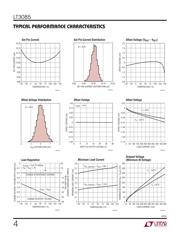
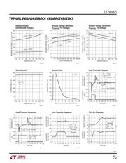
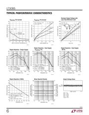
Performance Characteristics graphs for more information.
Note 10. This IC includes over-temperature protection that is intended
to protect the device during momentary overload conditions. Junction
temperature will exceed the maximum operating junction temperature
when over-temperature protection is active. Continuous operation above
the specifi ed maximum operating junction temperature may impair device
reliability.
器件 Datasheet 文档搜索
AiEMA 数据库涵盖高达 72,405,303 个元件的数据手册,每天更新 5,000 多个 PDF 文件
