Datasheet 搜索 > 运算放大器 > Linear Technology(凌力尔特) > LT6106CS5#PBF 数据手册 > LT6106CS5#PBF 数据手册 3/12 页

¥ 10.762
LT6106CS5#PBF 数据手册 - Linear Technology(凌力尔特)
制造商:
Linear Technology(凌力尔特)
分类:
运算放大器
封装:
TSOT-23
描述:
LINEAR TECHNOLOGY LT6106CS5#PBF 电流检测放大器, 高压侧, 1个放大器, 40 nA, TSOT-23, 5 引脚, 0 °C, 70 °C
Pictures:
3D模型
符号图
焊盘图
引脚图
产品图
页面导航:
导航目录
LT6106CS5#PBF数据手册
Page:
of 12 Go
若手册格式错乱,请下载阅览PDF原文件
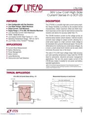
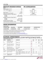
LT6106
3
6106fa
Note 1: Stresses beyond those listed under Absolute Maximum Ratings
may cause permanent damage to the device. Exposure to any Absolute
Maximum Rating condition for extended periods may affect device
reliability and lifetime. In addition to the Absolute Maximum Ratings, the
output current of the LT6106 must be limited to insure that the power
dissipation in the LT6106 does not allow the die temperature to exceed
150°C. See the applications information section “Power Dissipation
Considerations” for further information.
Note 2: Guaranteed by the gain error test.
Note 3: Gain error refers to the contribution of the LT6106 internal circuitry
and does not include errors in the external gain setting resistors.
Note 4: The LT6106C is guaranteed functional over the operating
temperature range of –40°C to 85°C. The LT6106C is designed,
ELECTRICAL CHARACTERISTICS
The ● denotes the specifi cations which apply over the full specifi ed
operating temperature range, otherwise specifi cations are at T
A
= 25°C. V
+
= 12V, V
+
= V
SENSE
+, R
IN
= 100Ω, R
OUT
= 10k, Gain = 100
unless otherwise noted.
SYMBOL PARAMETER CONDITIONS MIN TYP MAX UNITS
Minimum Output Voltage
(Note 5)
V
SENSE
= 0mV, R
IN
= 100Ω, R
OUT
= 10k
●
12 45
65
mV
mV
V
SENSE
= 0mV, R
IN
= 500Ω, R
OUT
= 10k, V
+
= 12V, 36V
●
716
22
mV
mV
BW Signal Bandwidth (–3dB) I
OUT
= 1mA, R
IN
= 100Ω, R
OUT
= 5k 200 kHz
t
r
Input Step Response (to 50% of
Output Step)
ΔV
SENSE
= 100mV Step, R
IN
= 100Ω, R
OUT
= 5k,
Rising Edge
3.5 μs
I
S
Supply Current V
+
= 2.7V, I
OUT
= 0μA, (V
SENSE
= –5mV)
●
60 85
115
μA
V
+
= 12V, I
OUT
= 0μA, (V
SENSE
= –5mV)
●
65 95
120
μA
V
+
= 36V, I
OUT
= 0μA, (V
SENSE
= –5mV)
●
70 100
130
μA
characterized and expected to meet specifi ed performance from –40°C to
85°C but is not tested or QA sampled at these temperatures. The LT6106H
is guaranteed to meet specifi ed performance from –40°C to 125°C.
Note 5: The LT6106 output is an open collector current source. The
minimum output voltage scales directly with the ratio R
OUT
/10k.
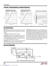
Note 6: V
SENSE
+
is the voltage at the high side of the sense resistor,
R
SENSE
. See Figure 1.
Note 7: V
SENSE (MAX)
is the maximum sense voltage for which the Electrical
Characteristics will apply. Higher voltages can affect performance but will
not damage the part provided that the output current of the LT6106 does
not exceed the allowable power dissipation as described in Note 1.
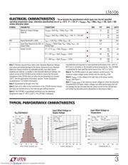
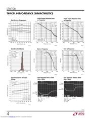
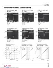
TYPICAL PERFORMANCE CHARACTERISTICS
Input Offset Voltage vs
Temperature
TEMPERATURE (°C)
–55
INPUT OFFSET VOLTAGE (μV)
0
200
125
6106 G03
–200
–400
–25 5
35 65
95
400
–100
100
–300
300
V
SENSE
= 5mV
V
+
= 12V
R
IN
= 100Ω
R
OUT
= 10k
A
V
= 100
TYPICAL UNITS
INPUT OFFSET VOLTAGE (μV)
–200
PERCENT OF UNITS (%)
10
12
16
120
6106 G23
4
8
14
6
2
0
–120
–40 0
40
200
V
+
= 12V
V
SENSE
= 5mV
R
IN
= 100Ω
R
OUT
= 10k
1068 UNITS
V
OS
Distribution
SUPPLY VOLTAGE (V)
0
CHANGE IN INPUT OFFSET VOLTAGE (μV)
10
40
50
40
6106 G02
0
–10
–70
10
20
30
5
15
25
35
–30
70
60
30
20
–20
–40
–50
–60
V
SENSE
= 5mV
R
IN
= 100Ω
R
OUT
= 10k
TYPICAL UNITS
Input Offset Voltage vs
Supply Voltage
Downloaded from Elcodis.com electronic components distributor
器件 Datasheet 文档搜索
AiEMA 数据库涵盖高达 72,405,303 个元件的数据手册,每天更新 5,000 多个 PDF 文件
