Datasheet 搜索 > ADI(亚德诺) > LTC1624IS8#PBF 数据手册 > LTC1624IS8#PBF 数据手册 5/28 页
 器件3D模型
¥ 0.587
LTC1624IS8#PBF 数据手册 - ADI(亚德诺)
制造商:
ADI(亚德诺)
封装:
SOP
描述:
升降压型 3.5V~36V 200kHz
Pictures:
3D模型
符号图
焊盘图
引脚图
产品图
页面导航:
引脚图在P4P5Hot
典型应用电路图在P1P5P13P21P22P23P24P25P26P27P28
应用领域在P1P5P7P8P9P10P11P12P13P14P15P16
电气规格在P3P4P9P11

导航目录
LTC1624IS8#PBF数据手册
Page:
of 28 Go
若手册格式错乱,请下载阅览PDF原文件

5
LTC1624
TG (Pin 6): High Current Gate Drive for Top N-Channel
MOSFET. This is the output of a floating driver with a
voltage swing equal to INTV
CC
superimposed on the
switch node voltage SW.
BOOST (Pin 7): Supply to Topside Floating Driver. The
bootstrap capacitor C
B
is returned to this pin. Voltage
swing at this pin is from INTV
CC
to V
IN
+ INTV
CC
in step-
down applications. In non step-down topologies the volt-
age at this pin is constant and equal to INTV
CC
if SW = 0V.
V
IN
(Pin 8): Main Supply Pin and the (+) Input to the
Current Comparator. Must be closely decoupled to ground.
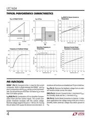
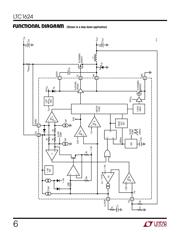
PIN FUNCTIONS
UUU
(Refer to Functional Diagram)
OPERATIO
U
Main Control Loop
The LTC1624 uses a constant frequency, current mode
architecture. During normal operation, the top MOSFET is
turned on each cycle when the oscillator sets the RS latch
and turned off when the main current comparator I
1
resets
the RS latch. The peak inductor current at which I
1
resets
the RS latch is controlled by the voltage on the I
TH
/RUN
pin, which is the output of error amplifier EA. The V
FB
pin,
described in the pin functions, allows EA to receive an
output feedback voltage from an external resistive divider.
When the load current increases, it causes a slight
decrease in V
FB
relative to the 1.19V reference, which in
turn causes the I
TH
/RUN voltage to increase until the
average inductor current matches the new load current.
While the top MOSFET is off, the internal bottom MOSFET
is turned on for approximately 300ns to 400ns to recharge
the bootstrap capacitor C
B
.
The top MOSFET driver is biased from the floating boot-
strap capacitor C
B
that is recharged during each off cycle.
The dropout detector counts the number of oscillator
cycles that the top MOSFET remains on and periodically
forces a brief off period to allow C
B
to recharge.
The main control loop is shut down by pulling the I
TH
/RUN
pin below its 1.19V clamp voltage. Releasing I
TH
/RUN
allows an internal 2.5µA current source to charge com-
pensation capacitor C
C
. When the I
TH
/RUN pin voltage
reaches 0.8V the main control loop is enabled with the I
TH
/
RUN voltage pulled up by the error amp. Soft start can be
implemented by ramping the voltage on the I
TH
/RUN pin
from 1.19V to its 2.4V maximum (see Applications Infor-
mation section).
Comparator OV guards against transient output over-
shoots >7.5% by turning off the top MOSFET and keeping
it off until the fault is removed.
Low Current Operation
The LTC1624 is capable of Burst Mode operation in which
the external MOSFET operates intermittently based on
load demand. The transition to low current operation
begins when comparator B detects when the I
TH
/RUN
voltage is below 1.5V. If the voltage across R
SENSE
does
not exceed the offset of I
2
(approximately 20mV) for one
full cycle, then on following cycles the top and internal
bottom drives are disabled. This continues until the I
TH
voltage exceeds 1.5V, which causes drive to be returned to
the TG pin on the next cycle.
INTV
CC
Power/Boost Supply
Power for the top and internal bottom MOSFET drivers is
derived from V
IN
. An internal regulator supplies INTV
CC
power. To power the top driver in step-down applications
an internal high voltage diode recharges the bootstrap
capacitor C
B
during each off cycle from the INTV
CC
supply.
A small internal N-channel MOSFET pulls the switch node
(SW) to ground each cycle after the top MOSFET has
turned off ensuring the bootstrap capacitor is kept fully
charged.
器件 Datasheet 文档搜索
AiEMA 数据库涵盖高达 72,405,303 个元件的数据手册,每天更新 5,000 多个 PDF 文件
