Datasheet 搜索 > AD转换器 > Linear Technology(凌力尔特) > LTC1864CS8#TR 数据手册 > LTC1864CS8#TR 数据手册 10/24 页

 器件3D模型
¥ 50.056
LTC1864CS8#TR 数据手册 - Linear Technology(凌力尔特)
制造商:
Linear Technology(凌力尔特)
分类:
AD转换器
封装:
SO-8
描述:
模数转换器 - ADC LTC1864 - - Power, 16-Bit, 250ksps 1- and 2-Channel ADCs in SOIC
Pictures:
3D模型
符号图
焊盘图
引脚图
产品图
页面导航:
引脚图在P10Hot
典型应用电路图在P1P24
原理图在P11P16
封装尺寸在P23
焊盘布局在P21P22
型号编码规则在P3
标记信息在P3
封装信息在P3
技术参数、封装参数在P7
应用领域在P1P13P14P15P16P17P18P19P20
电气规格在P5P8P9
型号编号列表在P24

导航目录
LTC1864CS8#TR数据手册
Page:
of 24 Go
若手册格式错乱,请下载阅览PDF原文件

LTC1864/LTC1865
10
18645fb
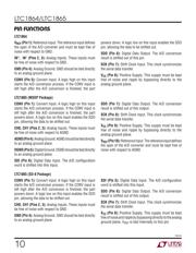
PIN FUNCTIONS
V
REF
(Pin 1): Reference Input. The reference input defi nes
the span of the A/D converter and must be kept free of
noise with respect to GND.
IN
+
, IN
–
(Pins 2, 3): Analog Inputs. These inputs must
be free of noise with respect to GND.
GND (Pin 4): Analog Ground. GND should be tied directly
to an analog ground plane.
CONV (Pin 5): Convert Input. A logic high on this input
starts the A/D conversion process. If the CONV input is
left high after the A/D conversion is fi nished, the part
powers down. A logic low on this input enables the SDO
pin, allowing the data to be shifted out.
SDO (Pin 6): Digital Data Output. The A/D conversion
result is shifted out of this pin.
SCK (Pin 7): Shift Clock Input. This clock synchronizes
the serial data transfer.
V
CC
(Pin 8):
Positive Supply. This supply must be kept
free of noise and ripple by bypassing directly to the
analog ground plane.
CONV (Pin 1): Convert Input. A logic high on this input
starts the A/D conversion process. If the CONV input is
left high after the A/D conversion is fi nished, the part
powers down. A logic low on this input enables the SDO
pin, allowing the data to be shifted out.
CH0, CH1 (Pins 2, 3): Analog Inputs. These inputs must
be free of noise with respect to AGND.
AGND (Pin 4): Analog Ground. AGND should be tied directly
to an analog ground plane.
DGND (Pin 5): Digital Ground. DGND should be tied directly
to an analog ground plane.
SDI (Pin 6):
Digital Data Input. The A/D confi guration
word is shifted into this input.
SDO (Pin 7): Digital Data Output. The A/D conversion
result is shifted out of this output.
SCK (Pin 8): Shift Clock Input. This clock synchronizes
the serial data transfer.
V
CC
(Pin 9):
Positive Supply. This supply must be kept
free of noise and ripple by bypassing directly to the
analog ground plane.
V
REF
(Pin 10): Reference Input. The reference input defi nes
the span of the A/D converter and must be kept free of
noise with respect to AGND.
LTC1864
LTC1865 (MSOP Package)
LTC1865 (SO-8 Package)
CONV (Pin 1): Convert Input. A logic high on this input
starts the A/D conversion process. If the CONV input is
left high after the A/D conversion is fi nished, the part
powers down. A logic low on this input enables the SDO
pin, allowing the data to be shifted out.
CH0, CH1 (Pins 2, 3): Analog Inputs. These inputs must
be free of noise with respect to GND.
GND (Pin 4): Analog Ground. GND should be tied directly
to an analog ground plane.
SDI (Pin 5):
Digital Data Input. The A/D confi guration
word is shifted into this input.
SDO (Pin 6): Digital Data Output. The A/D conversion
result is shifted out of this output.
SCK (Pin 7): Shift Clock Input. This clock synchronizes
the serial data transfer.
V
CC
(Pin 8):
Positive Supply. This supply must be kept
free of noise and ripple by bypassing directly to the analog
ground plane. V
REF
is tied internally to this pin.
器件 Datasheet 文档搜索
AiEMA 数据库涵盖高达 72,405,303 个元件的数据手册,每天更新 5,000 多个 PDF 文件
