Datasheet 搜索 > 放大器、缓冲器 > Linear Technology(凌力尔特) > LTC2050HVCS8#TR 数据手册 > LTC2050HVCS8#TR 数据手册 6/16 页
 器件3D模型
¥ 12.01
LTC2050HVCS8#TR 数据手册 - Linear Technology(凌力尔特)
制造商:
Linear Technology(凌力尔特)
分类:
放大器、缓冲器
封装:
SO
Pictures:
3D模型
符号图
焊盘图
引脚图
产品图
页面导航:
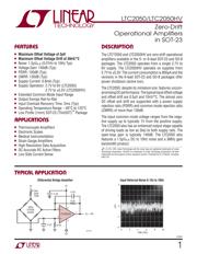
典型应用电路图在P1P11P12P16
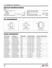
封装尺寸在P3P14P15
焊盘布局在P13P14P15
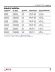
型号编码规则在P3
标记信息在P3
封装信息在P3
技术参数、封装参数在P6
应用领域在P1P10P11P12
电气规格在P4P5P6P7P8P9
导航目录
LTC2050HVCS8#TR数据手册
Page:
of 16 Go
若手册格式错乱,请下载阅览PDF原文件
LTC2050/LTC2050HV
6
2050fc
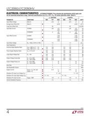
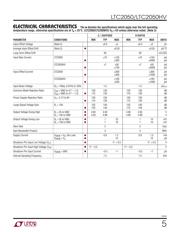
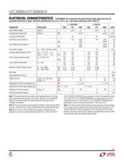
ELECTRICAL CHARACTERISTICS
(LTC2050HV) The l denotes the specifi cations which apply over the full
operating temperature range, otherwise specifi cations are at T
A
= 25°C. V
S
= ±5V unless otherwise noted. (Note 3)
PARAMETER CONDITIONS
C, I SUFFIXES H SUFFIX
UNITSMIN TYP MAX MIN TYP MAX
Input Offset Voltage (Note 2) ±0.5 ±3 ±0.5 ±3 μV
Average Input Offset Drift (Note 2)
l
±0.03 ±0.05 μV/°C
Long-Term Offset Drift 50 50 nV/√mo
Input Bias Current (Note 4)
l
±25 ±125
±300
±25 ±125
±4000
pA
pA
Input Offset Current (Note 4)
l
±250
±500
±250
±1000
pA
pA
Input Noise Voltage R
S
= 100Ω, 0.01Hz to 10Hz 1.5 1.5 μV
P-P
Common Mode Rejection Ratio V
CM
= V
–
to (V
+
– 1.3)
V
CM
= V
–
to (V
+
– 1.3)
l
120
115
130
130
120
115
130
130
dB
dB
Power Supply Rejection Ratio V
S
= 2.7V to 11V
l
120
115
130
130
120
115
130
130
dB
dB
Large-Signal Voltage Gain R
L
= 10k 125
120
140
140
125
120
140
140
dB
dB
Maximum Output Voltage Swing R
L
= 2k to GND
R
L
= 10k to GND
l
l
±4.75
±4.90
±4.94
±4.98
±4.50
±4.85
±4.94
±4.98
V
V
Slew Rate 2 2 V/μs
Gain Bandwidth Product 3 3 MHz
Supply Current V
SHDN
= V
IH
, No Load
V
SHDN
= V
IL
l
l
1 1.5
25
1 1.6
25
mA
μA
Shutdown Pin Input Low Voltage (V
IL
)
l
V
–
+ 0.5 V
–
+ 0.5 V
Shutdown Pin Input High Voltage (V
IH
)
l
V
+
– 0.5 V
+
– 0.5 V
Shutdown Pin Input Current V
SHDN
= V
–
l
–3 –20 –3 –20 μA
Internal Sampling Frequency 7.5 7.5 kHz
Note 1: Stresses beyond those listed under Absolute Maximum Ratings
may cause permanent damage to the device. Exposure to any Absolute
Maximum Rating condition for extended periods may affect device
reliability and lifetime.
Note 2: These parameters are guaranteed by design. Thermocouple effects
preclude measurements of these voltage levels during automated testing.
Note 3: All versions of the LTC2050 are designed, characterized and
expected to meet the extended temperature limits of –40°C and 125°C.
The LTC2050C/LTC2050HVC are guaranteed to meet the temperature limits
of 0°C and 70°C. The LTC2050I/LTC2050HVI are guaranteed to meet the
temperature limits of –40°C and 85°C. The LTC2050H/LTC2050HVH are
guaranteed to meet the temperature limits of –40°C and 125°C.
Note 4: The bias current measurement accuracy depends on the proximity
of the supply bypass capacitor to the device under test, especially at ±5V
supplies. Because of testing limitations on the placement of this bypass
capacitor, the bias current at ±5V supplies is guaranteed by design to meet
the data sheet limits, but tested to relaxed limits.
器件 Datasheet 文档搜索
AiEMA 数据库涵盖高达 72,405,303 个元件的数据手册,每天更新 5,000 多个 PDF 文件
