Datasheet 搜索 > 稳压芯片 > Linear Technology(凌力尔特) > LTC3736EGN-1#PBF 数据手册 > LTC3736EGN-1#PBF 数据手册 3/28 页
 器件3D模型
¥ 43.805
LTC3736EGN-1#PBF 数据手册 - Linear Technology(凌力尔特)
制造商:
Linear Technology(凌力尔特)
分类:
稳压芯片
封装:
SSOP-24
描述:
LINEAR TECHNOLOGY LTC3736EGN-1#PBF 直流/直流控制器, 电流模式, 2相, 2.75V至9.8V, 2路输出, 同步降压, 825kHz, SSOP-24
Pictures:
3D模型
符号图
焊盘图
引脚图
产品图
页面导航:
导航目录
LTC3736EGN-1#PBF数据手册
Page:
of 28 Go
若手册格式错乱,请下载阅览PDF原文件
3
LTC3736-1
37361f
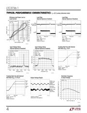
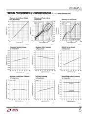
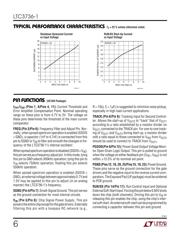
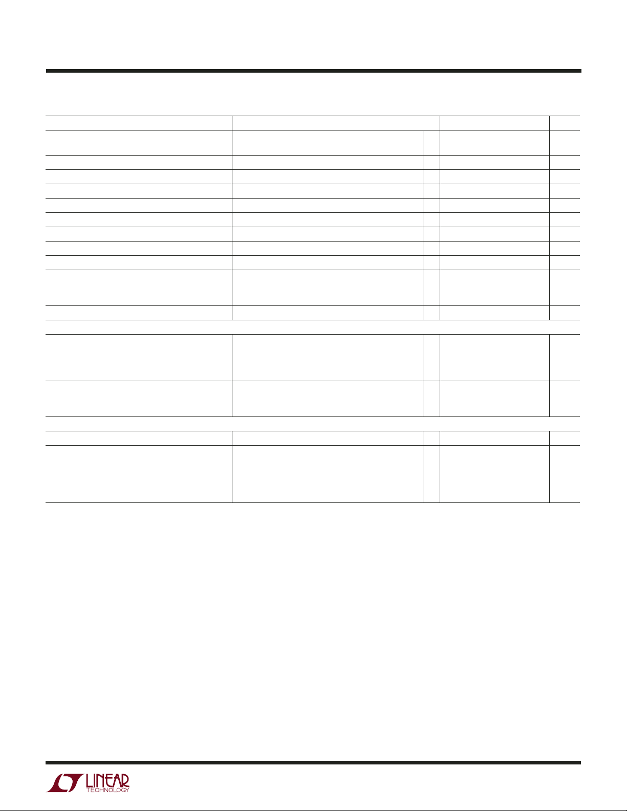
ELECTRICAL CHARACTERISTICS
The ● denotes specifications that apply over the full operating temperature
range, otherwise specifications are at T
A
= 25°C. V
IN
= 4.2V unless otherwise specified.
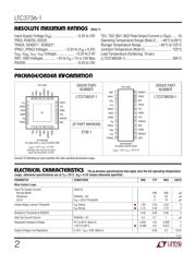
Note 1: Absolute Maximum Ratings are those values beyond which the life
of a device may be impaired.
Note 2: The LTC3736E-1 is guaranteed to meet specified performance
from 0°C to 70°C. Specifications over the –40°C to 85°C operating range
are assured by design, characterization and correlation with statistical
process controls.
Note 3: T
J
is calculated from the ambient temperature T
A
and power
dissipation P
D
according to the following formula:
T
J
= T
A
+ (P
D
• θ
JA
°C/W)
Note 4: Dynamic supply current is higher due to gate charge being
delivered at the switching frequency.
Note 5: The LTC3736-1 is tested in a feedback loop that servos I
TH
to a
specified voltage and measures the resultant V
FB
voltage.
Note 6: Peak current sense voltage is reduced dependent on duty cycle to
a percentage of value as shown in Figure 2.
PARAMETER CONDITIONS MIN TYP MAX UNITS
Output Voltage Load Regulation I
TH
= 0.9V (Note 5) 0.12 0.5 %
I
TH
= 1.7V –0.12 –0.5 %
V
FB1,2
Input Current (Note 5) 10 50 nA
TRACK Input Current TRACK = 0.6V 10 50 nA
Overvoltage Protect Threshold Measured at V
FB
0.66 0.68 0.7 V
Overvoltage Protect Hysteresis 20 mV
Top Gate (TG) Drive 1, 2 Rise Time C
L
= 3000pF 40 ns
Top Gate (TG) Drive 1, 2 Fall Time C
L
= 3000pF 40 ns
Bottom Gate (BG) Drive 1, 2 Rise Time C
L
= 3000pF 50 ns
Bottom Gate (BG) Drive 1, 2 Fall Time C
L
= 3000pF 40 ns
Maximum Current Sense Voltage IPRG = Floating (Note 6) ● 110 125 140 mV
(SENSE
+
– SW)(∆V
SENSE(MAX)
) IPRG = 0V ● 70 85 100 mV
IPRG = V
IN
● 185 204 223 mV
Soft-Start Time Time for V
FB1
to Ramp from 0.05V to 0.55V 0.667 0.833 1 ms
Spread Spectrum Oscillator
Oscillator Frequency Spread Spectrum Disabled (SSDIS = V
IN
)
V
FREQ
= Floating ● 480 550 600 kHz
V
FREQ
= 0V ● 260 300 340 kHz
V
FREQ
= V
IN
● 650 750 825 kHz
Spread Spectrum Frequency Range SSDIS = GND
Minimum Switching Frequency 450 kHz
Maximum Switching Frequency 580 kHz
PGOOD Output
PGOOD Voltage Low I
PGOOD
Sinking 1mA 125 mV
PGOOD Trip Level V
FB
with Respect to Set Output Voltage
V
FB
< 0.6V, Ramping Positive –13 –10.0 –7 %
V
FB
< 0.6V, Ramping Negative –16 –13.3 –10 %
V
FB
> 0.6V, Ramping Negative 7 10.0 13 %
V
FB
> 0.6V, Ramping Positive 10 13.3 16 %
器件 Datasheet 文档搜索
AiEMA 数据库涵盖高达 72,405,303 个元件的数据手册,每天更新 5,000 多个 PDF 文件
